Sunny superpower: solar cells close in on 50% efficiency

For solar cells, efficiency really matters. This crucial metric determines how much energy can be harvested from rooftops and solar farms, with commercial solar panels made of silicon typically achieving an efficiency of 20%. For satellites, meanwhile, the efficiency defines the size and weight of the solar panels needed to power the spacecraft, which directly affects manufacturing and launch costs.

To make a really efficient device, it is tempting to pick a material that absorbs all the Sun’s radiation – from the high-energy rays in the ultraviolet, through to the visible, and out to the really long wavelengths in the infrared. That approach might lead you to build a cell out of a material like mercury telluride, which converts nearly all of the Sun’s incoming photons into current-generating electrons. But there is an enormous price to pay: each photon absorbed by this material only produces a tiny amount of energy, which means that the power generated by the device would be pitiful.

Hitting the sweet spot

A better tactic is to pick a semiconductor with an absorption profile that optimizes the trade-off between the energy generated by each captured photon and the fraction of sunlight absorbed by the cell. A material at this sweet spot is gallium arsenide (GaAs). Also used in smartphones to amplify radio-frequency signals and create laser-light for facial recognition, GaAs has long been one of the go-to materials for engineering high-efficiency solar cells. These cells are not perfect, however – even after minimizing material defects that degrade performance, the best solar cells made from GaAs still struggle to reach efficiencies beyond 25%.

Further gains come from stacking different semiconductors on top of one another, and carefully selecting a combination that efficiently harvests the Sun’s output. This well-trodden path has seen solar-cell efficiencies climb over several decades, along with the number of light-absorbing layers. Both hit a new high last year when a team from the National Renewable Energy Laboratory (NREL) in Golden, Colorado, unveiled a device with a record-breaking efficiency of 47.1% – tantalizingly close to the 50% milestone (Nature Energy 5 326). Until then, bragging rights had been held by structures with four absorbing layers, but the US researchers found that six is a “natural sweet spot”, according to team leader John Geisz.

Getting this far has not been easy, because it is far from trivial to create layered structures from different materials. High-efficiency solar cells are formed by epitaxy, a process in which material is grown on a crystalline substrate, one atomic layer at a time. Such epitaxial growth can produce the high-quality crystal structures needed for an efficient solar cell, but only if the atomic spacing of each material within the stack is very similar. This condition, known as lattice matching, restricts the palette of suitable materials: silicon cannot be used, for example, because it is not blessed with a family of alloys with similar atomic spacing.

Devices with multiple materials – referred to as multi-junction cells – have traditionally been based on GaAs, the record-breaking material for a single-junction device. A common architecture is a triple-junction cell comprising three compound semiconductors: a low-energy indium gallium arsen­ide (InGaAs) sub-cell, a medium-energy sub-cell of GaAs and a high-energy sub-cell of indium gallium phosphide (InGaP). In these multi-junction cells, current flows perpendicularly through all the absorbing layers, which are joined in series. With this electrical configuration, the thickness of every sub-cell must be chosen so that all generate exactly the same current – otherwise any excess flow of electrons would be wasted, reducing the overall efficiency.

Bending the rules

Key to the success of NREL’s device are three InGaAs sub-cells that excel at absorbing light in the infrared, which contains a significant proportion of the Sun’s radiation. Achieving strong absorption at these long wavelengths requires InGaAs compositions with a significantly different atomic spacing to that of the substrate. Additionally, their device has been designed with intermediate transparent layers made from InGaP or AlGaInAs to keep material imperfections in check. Grading the composition of these buffer layers enables a steady increase in lattice constant, thereby providing a strong foundation for local lattice-matched growth of sub-cells that are not riddled with strain-induced defects.

The NREL team, which has pioneered this approach, advocates the so-called “inverted variant” structure. With this architecture, the highest energy cell is grown first, followed by those of decreasing energy, so that the cells lattice-matched to the substrate precede the growth of graded layers. This approach improves the quality of the device, while the fabrication process also results in the removal of the substrate – a step that could trim costs by enabling the substrate to be reused.
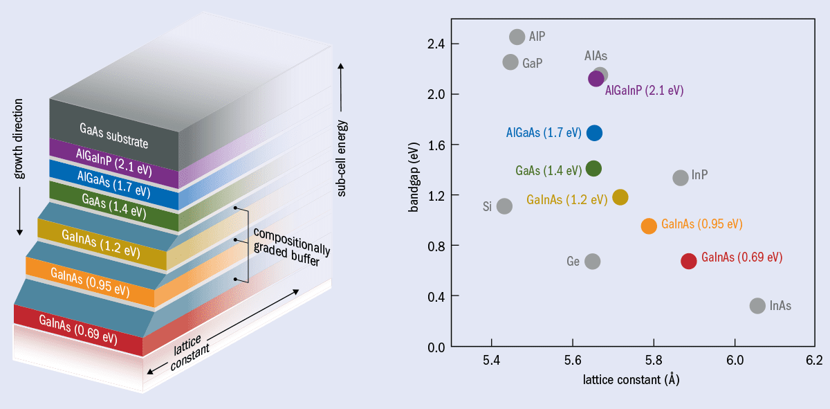
figure 1

One other technique that can further boost solar-cell efficiency is to focus sunlight on the cells, either with mirrors or lenses. The intensity of light on a solar cell is usually measured in “suns”, where one sun is roughly equivalent to 1 kW/m2. Concentrated sunlight increases the ratio of the current produced when the device is illuminated compared to when it is in the dark, thereby boosting the output voltage and increasing the efficiency. The gain is considerable: the NREL device achieves a maximum efficiency of just 39.2% when tweaked to optimize efficiency without any concentration, a long way short of the 47.1% record.

When Geisz and colleagues assessed how the performance of their six-junction cell varies with concentration, they found that peak efficiency occurs at 143 suns. Nevertheless, the device still produces a very impressive 44.9% efficiency at 1116 suns, which would generate a large amount of power from a very small device. As a comparison, a record-breaking cell operating at 500 suns could deliver the same power as a commercial solar panel from just one-thousandth of the chip area. At such high concentrations, however, steps must be taken to prevent the cell from overheating and diminishing performance.

Just over a decade ago, this approach to generating power from high-efficiency cells spawned a ­concentrating photovoltaic (CPV) industry, with a clutch of start-up firms producing systems that tracked the position of the Sun to maximize the energy that could be harvested from focusing sunlight on triple-junction cells. Unfortunately, this fledgling industry came up against the unforeseeable double whammy of a global financial crisis and a flooding of the market with incredibly cheap silicon panels produced by Chinese suppliers. The result was that so few CPV systems were deployed that even on a sunny day when all operate at their peak, their global output totals less than one-tenth of the power of a typical UK nuclear power station.

Extra-terrestrial encounters

Far greater commercial success for makers of multi-junction cells has come from powering satellites, most recently buoyed by the rollout of satellite broadband by companies such as OneWeb and Starlink. The key advantage here is that high-efficiency cells can drive down the costs of making and launching each satellite. As well as reducing the number of cells needed to power the spacecraft, higher efficiencies shrink both the size and weight of the solar panels that form the “wings” of the satellite. While launch costs have plummeted over the last few decades, satellite operators can still expect to pay almost $3000 per kilogram to get their spacecraft into orbit – and thousands of satellites are due to be deployed over the next few years.

For a solar cell in space, the crucial metric is the value at the end of its lifetime – after the device has been bombarded by radiation

However, for a solar cell in space, the crucial metric is not the initial efficiency but the value at the end of its intended lifetime after the device has been bombarded by radiation. Compound semiconductors hold up to this battering far better than those made from silicon. Early studies showed that the difference in efficiency of compound semiconductors rises with age from 25% to 40–60%, which ensured the dominance of triple-junction cells for space applications. Even so, the efficiencies of the best commercial cells for satellites remain limited to around 30–33%. This is partly because the solar spectrum beyond our atmosphere has a stronger contribution in the ultraviolet, where it is much harder to make an efficient cell, and partly because there are no concentrating optics to focus sunlight onto the cell.

To drive down the watts-per-kilogram of solar power in space, a US team working on a project known as MOSAIC (micro-scale optimized solar-cell arrays with integrated concentration) has been making a compelling case for CPV in space. The team points out that it should be relatively easy to orientate the solar panels on a satellite to maximize power generation with lenses in front of the cells shielding them from radiation. Concentrations must be limited to no more than around 100 suns, however, because cells in space cannot be cooled by convection, only by heat dissipation through radiation and conduction.

Focusing sunlight onto a high-efficiency cell

For CPV to have a chance of succeeding in space, the large and heavy solar modules used in early terrestrial systems must be replaced with a significantly slimmed-down successor. Technology pioneered by project partner Semprius, a now defunct CPV system maker, excels in this regard. The firm developed a process that uses a rubber stamp to parallel-print vast arrays of tiny cells, each one subsequently capped by a small lens.

The best results have come from stacking a dual-junction GaAs-based cell on top of an InP-based triple-junction cell separated by a very thin dielectric polymer. Current cannot pass through this polymer film, so separate electrical connections are made to extract the current from each cell independently. While this doubles the number of electrical connections, it eliminates the need for current matching between the two devices. Lifting this restriction gives greater freedom to the design, potentially enabling this approach to challenge the efficiency of NREL’s record-breaking device under high concentrations. Operating at 92 suns under illumination which mimics that in space, the team’s latest device, still to be fully optimized, has an efficiency of 35.5%.

Towards 50%

The NREL researchers know what they need to do to break the 50% barrier. The goal they are chasing is to cut the resistance in their device by a factor of 10 to a value similar to that found in their three- and four-junction cousins. They are also well aware of the need to bring down the cost of producing such complex multi-junction cells.

Also chasing the 50% efficiency milestone is a team led by Mircea Guina from Tampere University of Technology in Finland. Guina and colleagues are pursuing lattice-matched designs with up to eight junctions, including as many as four from an exotic material system known as dilute nitrides – a combination of the traditional mix of indium, gallium, arsenic and antimonide, plus a few per cent of nitrogen.

Dilute nitrides are notoriously difficult to grow. Back in the 1990s, German electronics powerhouse Infineon developed lasers based on this material, but they were never a commercial success. More recently, Stanford University spin-off Solar Junction showcased the potential of this material in solar cells. Although the start-up went to the wall when CPV flopped, devices produced by the company grabbed the record for solar efficiency in 2011 and raised it again in 2012 with triple-junction designs. Guina and co-workers are well positioned to take their technology further. They have made progress in producing all four of the dilute nitride sub-cells needed to produce record-breaking devices, and their efforts are now focused on optimizing the high-energy junction. The team’s work has been delayed due to the COVID-19 pandemic, but Guina believes that the approach could break the 50% barrier, possibly raising the bar as high as 54%.

There is still a question of impetus, however. The lack of commercial interest in terrestrial CPV may well encourage Guina to change direction and focus on chasing the record for space cells with no concentration. Much of today’s multi-junction solar-cell research is not focusing on power generation here on Earth, so while that 50% milestone is tantalizingly close, it might not be broken anytime soon.


Probing the gelation of egg whites with X-ray scattering

New research shows that the humble egg white could hold the answer to a long-standing mystery about the evolution of gels. In a paper published in Physical Review Letters, scientists at the University of Tübingen led by Frank Schreiber used ultrasmall angle X-ray scattering to show that cooked egg white is dynamic gel that continues to evolve long after solidifying. They attribute the unusual dynamics to rupturing of protein bonds and show that these events are highly correlated. This research has profound implications both for the food industry and the fundamental study of phase transitions.

Cheese, coagulated blood and cooked egg white are all common examples of gels. Though they behave as solids, these materials are mostly liquid; rigidity is imposed by a “skeleton” of solid particles that spans the material in a branched network. Egg whites, for example, start out as proteins swimming around in water, but heat forces them to unfurl and stick together, triggering gelation.

Gels exist out of equilibrium and so continue to evolve by relaxing into lower energy states long after the gelation transition. The group in Tübingen was motivated by a long-standing debate over whether the ageing of gels progresses continuously or via sudden intermittent rupturing of particle bonds. There was no research on the ageing of protein gels because of the challenge posed by studying structures without a single characteristic length scale; it is not clear whether the basic building block of a gel is the individual proteins or the long chains. In fact, the full dynamics can only be captured by studying the gel simultaneously at length scales of both the diameter of a few proteins and the length of the branches in the network (hundreds of nanometres to microns)

X-ray photon correlation spectroscopy (XPCS) is a technique that measures correlation between scattered photons. It is widely used to measure the dynamics of disordered materials but in its conventional configuration would only measure the motion of individual proteins. The researchers adapted XPCS for studying gel dynamics by combining it with ultrasmall-angle X-ray scattering, a state-of-the-art technique that probes up to large length scales.

Separating structure and dynamics

Schreiber and his colleagues performed XPCS on a sample of egg white as it was heated and observed the growth of a branched network structure. The structural evolution of the gel appeared at first to be incompatible with ageing as the complexity of the network and the average size of the branches changed very little with time.

However, far from being static, the gel exhibited intermittent motion. This was too fast to be diffusion and instead indicated the sudden rupturing of the protein–protein bonds. Intriguingly, relative to their size, long chains were more dynamic than single proteins, a behaviour that seems to be unique to this system.

Stress redistribution

These length-scale-dependent dynamics disappear over time, which the researchers believe is a clue as to how the gel can be dynamic without its overall structure changing. Because it is disordered, unusually large stresses become locked into certain regions of the gel. They propose that the rupturing of bonds in these regions redistributes the stresses, reducing spatial fluctuations in the gel without changing its average structure. Over time, as the gel becomes homogeneous, the length-scale-dependent dynamics disappear, and the gel evolves via a larger number of smaller rearrangements.

The most striking dynamical behaviour of the gel was that as well as evolving with time, the bond- rupturing events were not independent. Periodic variation in the relaxation time of the gel was observed, this has not been seen before and indicates that the rearrangement events are correlated. Whether this is a particular property of egg whites or a universal gelation behaviour being observed for the first time is not yet clear. It indicates that the gel can be split into substructures; a “fast” gel that mediates bond rupturing and a “slow” gel that preserves the original structure during ageing.

Most research on gel ageing uses either synthetic particles or simulations, but it seems that not for the first time, nature is a more intuitive scientist than we are. On the significance of the research, Schreiber says, “In the future, this will allow us to understand dynamics of different biological macromolecules in a broader range and more fundamentally.” By applying physical principles to these systems, this research could bridge the gap between thermodynamics and biology.

Majorana-based quantum computation gets a handy new platform

The errors that arise from the volatile nature of quantum technologies are a major roadblock on the path to practical quantum computing. We can imagine getting past this blockade by driving straight through it, using a car built to withstand the impact: this is quantum error correction. Alternatively, we might try to drive around the obstacle, bypassing the original problem entirely. To that end, researchers are investigating Majorana fermions – curious quantum objects that are their own antiparticles and are thought to be naturally resilient to quantum errors. So far, however, these quantum objects have proven difficult to create and control.

Researchers at the University of Maryland, US have now identified a more experimentally feasible way to generate Majorana fermions, potentially paving the way for Majorana-based quantum computation. In a paper published in Physical Review Letters, they show that a simple physical system can serve as a flexible platform for observing and manipulating these particles. The platform’s utility derives from its simplicity, says Ruixing Zhang, a postdoctoral researcher at Maryland and lead author of the study. “We don’t have to create additional structures. Nature gives us everything we need,” he says.

Majorana modes pose major challenges

Majorana fermions are not single particles like the electron or the photon. Instead, they are a template for a certain type of particle. After the Italian physicist Ettore Majorana predicted their existence in 1937, physicists hoped that some elementary particles might fit this mould, but subsequent experiments ruled this out for all known particles except the neutrino.

More recently, the Majorana fermion has taken on new life in the confines of ultracold quantum systems. In this context, Majorana fermions can manifest as collective oscillations of electrons. These electronic undulations are called quasiparticles because they behave in many ways like elementary particles, but emerge from the intricate interplay of many particles. Majorana fermions of this type live on the edges of their host materials and are the starting point for generating so-called Majorana zero modes (MZMs), which have zero energy and are further localized as point objects. The MZMs, in turn, can be used to build naturally error-resistant qubits.

Majorana modes are, however, notoriously elusive. In part, this is because it is hard to create the conditions required to generate them in an experimental setting. Many theoretical proposals have predicted MZMs should be present in quasi-2D materials, which consist of a small number of 2D layers stacked on top of each other. However, all previous proposals required heterostructures – that is, structures where the stacked layers have differing material composition and structure. Practically, these heterostructures are difficult if not downright impossible to grow.

To make matters worse, Majorana modes can only be observed indirectly. Like detectives trying to catch a culprit with only circumstantial evidence, physicists have a hard time ruling out alternative explanations for the phenomena they observe. This has led to high-profile premature claims of Majorana discovery, including Microsoft Quantum Lab’s recent retraction of a Nature paper in which they purported to observe MZMs in nanowires.

Photo of Ruixing Zhang

Ironing out problems

In their new work, Zhang and his coauthor show that Majorana modes should be present in a much simpler setting: thin films of an iron-based superconducting material. Like previous proposals, the system they study is quasi-2D, but crucially all layers are of the same kind. The iron-based thin films naturally accommodate Majorana fermions that are helical – left or right-handed – and move along the edges of the system in their preferred direction. This is due to a special “time-reversal” symmetry, wherein interchanging the left-moving and right-moving quasiparticles makes it look like time is propagating backwards in the system.

With these thin films, making MZMs from helical Majorana fermions is relatively simple. When a magnetic field is applied to the system, the Majorana modes shift from being spread out around the edges of the system to localizing in its corners. Rotating the magnetic field has the effect of transporting each Majorana mode from one corner to another. This magnetic knob can be used to “braid” the Majoranas, which is the cornerstone for logic gates – controlled operations required to perform computation – in topological quantum computers.

At its core, Zhang’s analysis has real-world applications in mind. The thin films he studies can be grown one layer at a time using a technique known as epitaxy, and all of the essential ingredients that are mixed together to produce helical Majorana modes have been previously realized and observed experimentally. Zhang’s work also shows that an electric field, which is easy to apply experimentally, can serve as a “topological switch” for controlling the emergent quasiparticles.

What’s more, the researchers also propose a new “smoking gun” for confirming the presence of MZMs based on this corner localization. Traditional techniques, which involve analyzing the material’s transport properties, are experimentally challenging and have trouble disqualifying alternative explanations. Zhang’s new method, which centers around measuring the particle density across the thin film, is easier to implement, and facilitates catching the slippery suspects.

The road ahead

The path to large-scale quantum computing is protracted and precarious, but Zhang believes his work shows that it might be more feasible than previously thought to build a quantum computer out of Majorana modes – something that could help overcome the significant issue of quantum errors. “The first step is establishing the possibilities,” he says. “Next, we need to create a blueprint.”

Ships can monitor and predict ocean waves using new algorithm

The safety and efficiency of ocean-going vessels could soon get a boost from a new algorithm that can monitor and predict incoming ocean waves. Developed by a team led by Zhengru Ren at the Norwegian University of Science and Technology, the system relies only on information about the motions of ships, with no need for external sensor data. Their mathematical approach could benefit global maritime industries by being cheaper and more accurate than existing techniques.

Ocean waves hold a constant influence over the operation of ships, and the safety of their crews. To streamline the efficiency of maritime activities, operators must continually monitor surrounding “sea states”, which contain information about the heights, frequencies, and directions of incoming waves. This is often done using information from meteorological sensors including satellites and floating buoys. However, each of these measurement techniques has shortcomings, either relating to cost, or the real-time accuracy of their measurements.

Ren’s team introduce a more advanced approach in their method, which predicts future sea states based on real-time observations taken aboard a ship. In developing their algorithm, the researchers aimed for a “nonparametric” approach, which can reconstruct sea states based on their influence over a ship’s motion. This would be far more flexible than existing sensor-based methods, but would first require the team to apply several different mathematical techniques to ensure the best possible accuracy.

Bobbing up and down

To reconstruct surrounding sea states, a vessel’s motions are analysed using Fourier transforms, which gives “cross-spectra” of how the ship bobs up and down. Ren’s team then applied a smoothing function called a Bézier surface; before incorporating an optimization technique to minimize any errors originating from a vessel’s unique responses to waves.

Finally, the researchers applied pre-calculated functions named “response amplitude operators”, which can account for the unique geometries of ship hulls. This enabled their calculations to accurately represent the relationship between vessel motions and specific wave heights. With these combined techniques, Ren and colleagues could faithfully reconstruct the motions of incoming waves, based purely on the motions of a simulated ship.

Without any need to carefully tune the parameters of a model, ship operators could drastically reduce both the time and cost required to monitor surrounding sea states. These advantages are enhanced even further since the techniques can be readily applied in real-time scenarios, without any external sensors. Ren’s team now hopes that their algorithm could soon be widely implemented: improving both the safety and efficiency of shipping industries worldwide.

The algorithm is described in Marine Structures.

Deep learning helps doctors predict gastric cancer metastasis

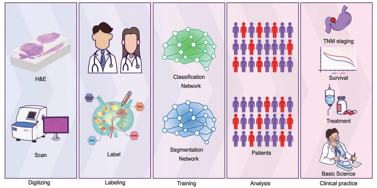
Research workflow

Early detection of metastasis, in which cancerous cells spread through the body, could turn the tide on cancer and enable clinicians to provide suitable therapies. Importantly, the introduction of artificial intelligence (AI) and enhanced image analysis has helped improve diagnostic accuracy. To assist pathologists in identifying metastatic lymph nodes (MLNs), researchers at Xidian University and Changhai Hospital in China have developed a computational approach to predicting the clinical outcomes of patients with gastric cancer.

Stomach cancer, also known as gastric cancer, occurs when cells in the inner lining of the stomach begin to grow abnormally. If left untreated for several years, these abnormal cells may develop into a tumour. Traditionally, experienced pathologists examine excised lymph nodes for the presence of gastric cancer metastases and evaluate the tissue morphology with the aid of an optical microscope. While this is an acceptable standard of practice, the process can be tedious and may lead to human errors.

The multidisciplinary group, led by Guanzhen Yu and Xiyang Liu, developed a deep-learning framework for identifying and analysing micrometastases (with a diameter of less than 2 mm) in lymph nodes. The framework was designed to uncover the tumour-area-to-MLN-area ratio (T/MLN) from whole slide images. The team tested the approach on two independent datasets of gastric cancer patients.

Diagnostic accuracy with AI assistance

The researchers point out that while pathologists possess better specificity in the detection of tumour tissues, AI offers scalability of performance due to its sensitivity and speed. Combining the two could provide the most clinically meaningful outcome.

The researchers first digitized MLN pathology samples and annotated them to create a training dataset. They then subjected this dataset to a deep-learning algorithm for classification and segmentation. These steps resulted in a precise calculation of the proportions of tumour components and lymph nodes in the samples.

Clinical pathologists reviewed the deep-learning results and reported a 94.5% consistency in lymph node detection between the AI diagnosis and the original diagnosis. Importantly, the researchers demonstrated that, with AI assistance, a pathologist required an average of 2–6  min to diagnose a patient’s lymph node. Without AI assistance, the diagnosis required 3–15 minutes.

This potential to enhance performance with AI-assisted analysis will improve patient prognosis and shorten the time required for making therapeutic decisions, say the researchers, who report their findings in Nature Communications.

Gastric cancer prediction

One challenge when predicting cancer prognosis is the insufficient information acquired during diagnostic evaluation. However, the deep-learning architecture developed in this study was able to efficiently identify MLNs, thereby reducing the rate of missed diagnosis by human pathologists. The researchers note that cancer patient’s outcomes were correlated with the area of metastatic tumour in the MLN. They could therefore use the AI algorithm to calculate the precise number of tumour cells within the MLN and deploy this as a prognostic marker for gastric cancer.

Prediction results

The researchers point out that the prediction results in this study are representative of a gastric cancer cohort from an individual nation. However, they propose that the AI should be tested in a large-scale clinical trial across several countries. They believe that this would validate the algorithm and enable clinicians to improve treatment outcomes.

Ultrasound detector uses optomechanical silicon photonics to boost sensitivity by 100 times

A highly sensitive optomechanical ultrasound detector integrated onto a silicon photonic chip has been developed by researchers in Belgium and Germany. The team, led by Wouter Westerveld at the Interuniversity Microelectronics Centre (IMEC) in Leuven, showed that its device is 100 times more sensitive than state-of-the-art piezoelectric detectors of identical sizes. Their design could substantially improve the performance of ultrasound detectors in a wide variety of biomedical applications.

Arrays of up to 10,000 piezoelectric ultrasound detectors are widely used to build up non-invasive images of living tissues. Unfortunately these detectors have three major limitations. First, there is a fundamental trade-off between the sizes and sensitivities of each sensor element – the smaller the element, the lower the sensitivity. This makes them unsuitable for the large, intricate arrays required to obtain low-noise, high-resolution ultrasound images.

Second, these sensors rely on mechanical resonance at specific ultrasound wavelengths to enhance the amplitude of their signals – restricting the devices to a narrow range of operational wavelengths. Finally, each sensor in the array requires its own electrical wire to transmit its signal to a computer, significantly driving up the cost of large detectors.

Split-rib waveguide

In this latest study, Westerveld’s team overcame each of these challenges using a new optomechanical ultrasound sensor (OMUS). Their design was based on a “split-rib” silicon photonic waveguide: containing a main part, attached to a moveable membrane; and a thinner “rib”, attached to a fixed substrate. This part of the waveguide was arranged in a ring shape, causing it to act as a photonic resonator. Both parts were separated by a tiny gap just 15 nm across, which contained an intense electric field.

When an ultrasound wave distorted the membrane even slightly, the electric field generated a large change in the waveguide’s refractive index – altering the resonant wavelength of the ring-shaped rib in turn. Using a tuneable laser, the researchers could then read out this wavelength in real time, producing a highly accurate signal.

Silicon integration

Westerveld’s team determined that an OMUS measuring 20 µm across is over 100 times more sensitive to ultrasound waves than an identically-sized piezoelectric counterpart. In addition, the sensors could be operated over a broad range of ultrasound wavelengths; while the signals produced by multiple devices could be read out using a single optical fibre. Taking advantage of these improvements, the researchers demonstrated how large, low-cost OMUS arrays could be integrated onto a silicon photonic chip.

The team describe its sensor as a game changer for deep tissue imaging. With such a low ultrasound detection limit, the OMUS is highly suitable for biomedical applications including mammography and tumour detection. It could even be used in miniaturized catheters, and to carry out non-invasive brain imaging through the skull – which was highly impractical in the past, due to the strong ultrasound attenuation of bone.

The research is described in Nature Photonics.

Advanced X-ray imaging creates sound-frequency maps of the human inner ear

Have you ever wondered how auditory information is transmitted from the inner ear to the brain? What about where exactly in the inner ear this takes place? Thanks to work by a research collaboration between Uppsala University and Western University, this is now possible.

Using a novel imaging technique called synchrotron radiation phase-contrast imaging (SR-PCI), the team has performed the first three-dimensional frequency analysis of the human cochlea, showing where the various sound frequencies are captured.

The human cochlea is a spiral structure of the inner ear. Sound vibrations are transmitted to the cochlea and then transduced into electrical activity along the basilar membrane (BM). The BM is a soft-tissue structure that categorizes different acoustic vibrations based on their frequency and produces a spatial frequency map in the cochlea.

Since the late 1990s, researchers have attempted to image the fine structures of the human inner ear using synchrotron radiation, but the technique could not resolve the boundaries between the BM and the rest of the cochlea. To overcome this, one solution was to use contrast agents for better soft-tissue visualization; however, non-uniform distribution of contrast and tissue shrinkage caused problems. And while other researchers have used SR-PCI, they could not develop complex 3D frequency maps of the cochlea. Although some attempted 3D reconstruction from two-dimensional histological sections, the process was laborious and prone to artefacts.

The working principle

Now, the research collaboration – led by Helge Rask-Andersen at Uppsala University and by Hanif Ladak and Sumit Agrawal at Western University – has successfully created a three-dimensional representation of sound-frequency mapping in the human cochlea, using SR-PCI to image adult human cadaveric cochlea. The team performed the SR-PCI study at the Canadian Light Source in Saskatoon, publishing the results in Scientific Reports.

The authors

SR-PCI is unique because it can enhance soft-tissue contrast while minimizing artefacts that may be introduced through staining, sectioning and decalcification in histopathology. In SR-PCI, varying material properties within the sample cause phase shifts that are then transformed into detectable variations in X-ray intensity. These variations can help to provide edge contrast to highlight soft tissues.

The new 3D cochlear model shows where the various frequencies of sound are captured and reveals the detailed anatomical structure of the intact cochlea. This offers many advantages. First, accurate tonotopic frequency distributions could result in improved surgical outcomes for cochlear implant recipients. In addition, this new knowledge could help to better individualize the programming of cochlear implants for future patients, so that each area in the ear can be stimulated with the correct frequency. This will help to improve the sound quality for cochlear implant users.

First author Hao Li

CZT detector technology: ready to shine in next-generation medical imaging systems

H3D is a US technology and research-focused business that provides high-performance imaging spectrometers for real-time identification and localization of gamma-ray sources. Over the past decade, the Ann Arbor, Michigan-based manufacturer has made its name serving a diverse base of end-users with specialist measurement solutions for gamma-ray imaging and spectroscopy. That customer base includes government agencies and nuclear first-responders, radiation safety officers at nuclear power plants, and international inspectors tasked with safeguarding and compliance in accordance with nuclear non-proliferation treaties.

“Our commercial instruments are based around cadmium zinc telluride (CZT) radiation detectors – a technology that combines industry-leading energy resolution and spatial resolution with room-temperature operation,” explains Willy Kaye, founder and CEO of H3D. As well as 10 full-time, PhD-level staff working on CZT device development and optimization, H3D draws on a broader pool of engineering and technical talent across the regional supply chain – most notably the Detroit car industry. “The emphasis at H3D is on robust, fully integrated radiation measurement solutions ready for field deployment,” Kaye adds. “To make this possible, we leverage expertise from a range of industry partners to ensure best practice in areas like manufacturability, packaging, mechanical testing, control electronics and software.”

The logic of diversification

If that’s the back-story, the next chapter in H3D’s development is already taking shape, building on those solid foundations to address CZT growth opportunities in the medical imaging market. Front-and-centre in H3D’s diversification effort is the M400 Series, a compact and customizable module capable of high-resolution gamma spectroscopy in a range of medical imaging applications. “The M400 is an off-the-shelf commercial product that can be easily ‘tiled’ to form imaging arrays with enhanced sensitivity,” says Kaye. “We anticipate broad applicability across multiple imaging modalities and clinical use cases.”

Right now, H3D’s engagement with the medical imaging community manifests in a targeted programme of R&D collaboration. It looks like a win-win: proof-of-concept experimental projects allow H3D engineers to gather custom requirements at scale, while simultaneously educating medical imaging specialists about the versatility and capability of CZT technology. One such collaboration is with the Maryland Proton Treatment Center in Baltimore. This six-year R&D effort, funded by the US National Institutes of Health (NIH), is evaluating the potential of CZT imaging in proton cancer therapy, an advanced form of radiotherapy that allows precise radiation delivery to complex tumour volumes while sparing healthy tissue and organs-at-risk.

Specifically, the M Series forms the basis of a high-energy, high-flux spectrometer that’s able to image high-energy gamma rays produced during proton therapy (the spectrometer being tiled up with 16 M400 units – i.e. 64 CZT crystals and a total crystal volume of 310 cm3). Although this is still early-stage evaluation work, the long-term objective is an on-board imaging system to ensure that the bulk of the radiation payload from the proton treatment beam is deposited into the tumour rather than adjacent healthy tissue.

Hao Yang

“The prompt gamma-ray emissions from proton interactions with tissue can be used to monitor the proton beam in vivo, providing real-time knowledge of tumour location, beam position, and beam penetration depth during treatment,” explains Hao Yang, a product development engineer at H3D.

“Worth noting,” he adds, “that the readout system is optimized for the high-flux conditions of proton cancer therapy, though ultimately it’s the system integration aspects that will be key to successful commercial engagement with the proton therapy OEMs.”

Functional imaging

In a separate collaboration, H3D engineers are investigating opportunities in small-animal positron emission tomography (PET), a functional imaging technique that uses radioactive tracers to track changes in the metabolism of diseased tissue (e.g. cancerous tumours) and physiological processes such as blood flow and chemical absorption. As such, small-animal PET provides a key imaging modality for the preclinical evaluation of new drugs, allowing biomedical scientists to track a drug’s behaviour over time versus a range of metrics such as treatment efficacy, biodistribution, toxicity and excretion. These small-animal studies, in turn, inform the regulatory approvals process ahead of advanced clinical trials in human patients.

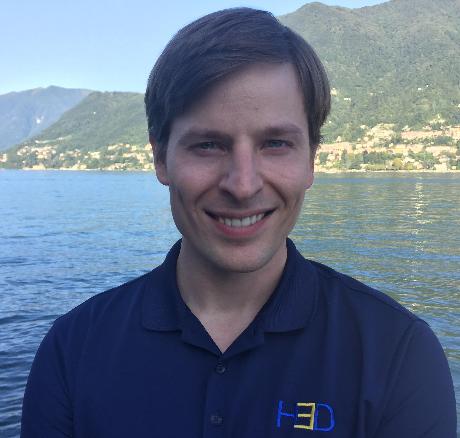
Willy Kaye

With this in mind, H3D has developed a prototype imaging detector (based on four specially arranged M400 modules) for applications in small-animal PET studies. The custom system, which is currently being evaluated by researchers at the University of Illinois at Urbana-Champaign, is capable of achieving 0.5 mm spatial resolution (versus 1 mm for the best commercial scintillators). “This is a significant step forward for small-animal PET and the best positional resolution of any traditional PET detector,” claims Kaye. Separately, the Urbana-Champaign scientists have also purchased 50 M400 modules to evaluate novel detector arrays for next-generation functional imaging systems.

Another application of interest for H3D is the monitoring of radioisotope distribution within the body during diagnostic or therapeutic medical procedures. The gamma-emitting technetium-99m, for example, is used for functional imaging of the skeleton and a range of organs (including the heart, liver, kidney and gall bladder), while iodine-131 is widely deployed for the treatment of an overactive thyroid gland or as a post-surgical follow-up when treating thyroid cancer.

In this scenario, H3D’s gamma-ray imaging spectrometers enable clinicians to validate their organ transport models for radiopharmaceuticals by providing precision overlay of gamma and optical images of the patient in real-time. “While we are confident that we have developed a truly unique measurement tool,” concludes Kaye, “as sensor developers we will need to rely on the creativity of our potential partners to figure out how to improve patient outcomes based on this technology.”

Product focus: the M400 Series

Versatile by design

H3D’s M400 Series is a custom integrable CZT detector module for high-resolution gamma spectroscopy and imaging. The product, which can be used as a single detector or tiled together for increased sensitivity, is suitable for a range of OEM system applications including drones, robots and medical imaging arrays. Technical specifications include:

  • Spatial resolution: <0.5 mm (≥140 keV)
  • Energy resolution: ≤1.1% FWHM at 662 keV (coincident interactions combined); enhanced resolution version also available (≤0.8% FWHM at 662 keV)
  • Crystal volume: >19 cm3 CZT (484 detector pixels)
  • Spectroscopy range: 50 keV to 3 MeV
  • Compton imaging range: 250 keV to 3 MeV (optional)
  • Dimensions: 10.2×5.3×5.3 cm and 0.6 kg

Free-space laser link beats the stability of optical clocks

Physicists in Australia have demonstrated how to create an exceptionally stable laser link to send frequency information through the atmosphere. The researchers say that fluctuations in the laser’s frequency are so minuscule that after just a few seconds of averaging such a link could be used to flawlessly transmit timing signals from the world’s most accurate optical clocks. This, they argue, offers the prospect of a global timing network that uses satellites to synchronize optical frequencies between continents.

This ability to connect optical clocks globally could potentially allow physicists to test general relativity, search for dark matter and detect any variabilities in the fundamental constants. It might also be used to improve satellite-based navigation and timing, as well as geodesy – thanks to the effects of gravitational time dilation at varying altitudes.

Optical clocks can now achieve uncertainties about 100 times lower than microwave-frequency, caesium-based atomic clocks – at roughly 1 part in 1018 – while their frequencies have been compared by linking them through optical fibre at distances of up to nearly 2000 km. But extending such comparisons across the globe will be tough, given the huge cost of laying a dedicated fibre with suitable amplifiers. Satellite radio links, on the other hand, are fine for microwave clocks but are orders of magnitude too imprecise for optical timekeepers.

As David Gozzard, Lewis Howard and colleagues at the University of Western Australia in Perth explain in a preprint uploaded to the arXiv server, any link must have a more stable frequency than the optical clocks they connect. Otherwise, the supreme accuracy of those clocks will go to waste. Stability can be raised by averaging a signal over a longer times, but that time is very limited – with some experts anticipating that optical clocks might soon become stable to one part in 1018 after running for just 100 s.

Atmospheric turbulence

The challenge for developers of free-space links is overcoming atmospheric turbulence. Fluctuations in the refractive index along the path of the laser slightly speed up or delay the light’s arrival, leading to phase instability. What is more, turbulence also causes the beam to wander off target and scintillate. This diminishes the beam intensity very briefly but repeatedly, with the loss of signal limiting the averaging time and with it the frequency stability.

To demonstrate how to overcome these problems, Gozzard and colleagues set up a laser transmitter and receiver on the rooftop of their university’s physics department. They then measured the stability of a beam bounced off a corner-cube reflector on another roof 1.2 km away. That 2.4 km horizontal round trip, they say, had about the same level of turbulence as would a link established between the ground and a satellite about 500 km up in a low-Earth orbit.

To maximize the system’s stability, the researchers were able to continually realign the reflected beam using a “tip-tilt” mirror moving in response to the fluctuating output from a photo detector that could capture intensity drops lasting less than a millisecond. In tandem, they used a phased-locked loop together with an acoustic-optic modulator to shift the light’s frequency.

Free-space attempts

This is not the first attempt to stabilize frequency transfers in free-space. The Australian group and colleagues in France reported in January having achieved a stability of 1.6 parts in 1019 after just 40 s of averaging. This compares well with 6 × 10-19 after about 30 h averaging, reported last year by researchers at the National Institute of Standards and Technology in the US when using a 1.5 km open-air link with optical clocks at either end. A group at the Korea Advanced Institute of Science and Technology has also carried out similar measurements on an 18 km open-air link.

However, the latest work pushes up stability significantly. Carrying out their experiment for two weeks in September 2020, Gozzard and colleagues found that the phase stabilisation technology alone allowed a fractional stability of 1 × 10−19 after averaging for a minute. By also stabilizing the amplitude, they were able to reduce signal loss and raise the stability to about 6 × 10−21 after 5 min. As they point out, this happens to be about the length of time that contact can be maintained with a satellite in low Earth orbit.

They then worked out what these figures would mean when linking up with a satellite in orbit. They found that the lower signal bandwidth due to the greater distance would slightly lower stabilities but still keep the system extremely competitive with the best optical clocks. They calculate that frequency comparisons would be limited by the clocks’ own instabilities after just a few seconds of averaging.

To test the technology for real, Gozzard and his colleagues are currently building a 0.7 m telescope on the ground and are hoping to get access to a satellite from either the French space agency CNES or a private company. He points out that they will have to contend with quite severe Doppler shift – a satellite’s movement towards and away from the ground station will cause the incoming signal to abruptly rise and fall by about 10 GHz. But he reckons that experience gained by the team dealing with high-precision microwave shifts on the Square Kilometre Array radio telescope should help them maintain current precision. “We’re confident we can adapt to the Doppler shift,” he says.

Promethean Particles spins out continuous process for making nanoparticles

Promethean Particles produces nanoparticles using a technique called hydrothermal synthesis; how does this process work?

Hydrothermal just means hot water. If you ever made a crystal garden when you were younger, you know that it involves dissolving large amounts of coloured metal salts in a small jar of water. What this does is create a super-saturated solution where the metal ions are ready to effectively “crash out” at the first opportunity. Put a piece of string into this solution and impressive-looking crystals grow onto the string over the next few days or weeks.

Hydrothermal synthesis has been used for hundreds of years to make large crystals (on long timescales) using a very similar process but in large batch autoclaves. In contrast, our crystallization process takes seconds because we are only growing nanocrystals, which are very small clusters of atoms, maybe 100 to 10,000 atoms in size. The nucleation of these particles is instantaneous and occurs in a continuous flow process. This flow process is designed to create a super-saturated solution just for the briefest moment, allowing nanoparticles to form.

How did you develop and commercialize the process?

The original idea for our continuous process came from Japan in the early 1990s, when a very well-known academic called Tadafumi Adschiri described a continuous process using two flows (a very hot flow and a cold flow containing the dissolved metal salts) introduced together in a high pressure T reactor arrangement. At first, we struggled to make nanoparticles in a way that avoided blockages. It took a few years to solve this problem because it was tricky to understand what was happening inside our steel reactor during the high-temperature, high-pressure process.

Once we perfected the process and reactor design, we filed a patent and started generating interest from companies that might want to take it forward. Eventually we took the step to commercialize the technology ourselves and formed Promethean Particles at the end of 2007. The route to commercialization is always an interesting one and the choice of whether to license intellectual property or create a spin-out company is one that academics with good ideas must wrestle with.

The choice of whether to license intellectual property or create a spin-out company is one that academics with good ideas must wrestle with

Did you get guidance from the University of Nottingham when making that decision?

Like most universities, Nottingham has a tech transfer office, and we discussed the possibility of a spin-out with them. We had a market survey commissioned to try to understand the potential marketplace for our products. The results were overwhelmingly positive, and so this gave us the initial confidence that there was a market for this technology.

In particular we discovered that industrial users of nanomaterials were frustrated with the quality of the nanoparticles they were buying and the lack of available industrial scale for other nanoparticles they would otherwise be interested in. One of the key things we offer our customers is the ability to enable them to achieve production scale. It was clear that we could meet their needs in different market sectors from coatings to medical applications, but the technology needed developing and scaling up to meet industrial demand. This positioning was key to our decision to spin out the technology rather than to license it.

Promethean Particles opened a manufacturing facility in Nottingham in 2016. What type of nanoparticles do you make there and what are they used for?

The first products that we made were ceramics – metal oxides that can be used in reflective coatings, high-temperature materials, catalysts or as strengthening materials for fabrics. Today, we can make materials in eight different materials classes including metals, metal oxides and metal-organic frameworks. Furthermore, within some of those classes, (e.g. doped metal oxides) there is a virtually limitless combination of materials that we can produce. These can be used in everything from batteries to anti viral coatings.

We produce both standardized and bespoke materials. We work closely with our customers to understand their needs and take them through our new product development process that first designs the nanomaterial solution, then develops it so it can be scaled, before delivering them the products that they are looking for.

We can make materials in eight different materials classes including metals, metal oxides and metal-organic frameworks

Can you give a flavour of some of the products you are currently working on?

We are working in several different market sectors and we have a few products that are either in or close to market.

We are working on a product that stops ice from building up on aeroplanes. Currently, de-icing is an expensive, time-consuming process that can lead to flight delays. It is done by spraying chemicals on aircraft, which removes ice and creates a temporary coating that prevents ice from forming – but nanoparticles could offer a better, more sustainable route to keeping the outside of the plane ice free. Nanomaterials are already used in exterior coatings to help aeroplanes fly more efficiently. By altering the morphology of these particles and their surface chemistry, we can stop water molecules building up and prevent the formation of ice. Essentially, this is the creation of a textured super-hydrophobic coating, which is also how self-cleaning glass works.

Because of the COVID-19 crisis, there has been great interest in the antiviral and antimicrobial additives that we can produce. We have been developing copper and silver nanoparticle-based inks for printing circuit boards, but it turns out that these metallic nanoparticles are also very good at killing the COVID-19 virus. We have other healthcare/PPE applications that are currently undergoing testing. Healthcare has become a much bigger thing for us in the past year.

We also get a lot of interest in our metal-organic frameworks (MOFs), which are porous materials that have an extremely high surface area. Indeed, a sample of MOFs powder that you can hold in your hand has the same surface area as an office block. This property means these MOFs can be used for gas storage, gas capture or chemical filtration.

We also make a dispersion that can be used as a thermal fluid to improve the efficiency of heating and cooling systems including air conditioning units. Reducing energy consumption is a key sustainability goal. More efficient heating and cooling systems would make a significant difference to global energy demand.

Copyright © 2026 by IOP Publishing Ltd and individual contributors