Einstein’s general theory of relativity has triumphed once again after being tested in the strongest gravitational field to date. Dimitrios Psaltis at the University of Arizona and members of the Event Horizon Telescope (EHT) collaboration did their analysis using recent images of M87*, which is a supermassive black hole at the centre of a nearby galaxy. Their results set the stage for even more stringent tests of general relativity in the near future.
For over a century, general relativity has had an excellent track record in explaining observations of the universe. All the same, the theory leaves some big questions unanswered: including how to unify gravity with quantum mechanics and the surprise discovery in 1998 of the universe’s accelerating expansion. As a result, physicists are looking for subtle flaws in general relativity that could lead to the development of a more complete theory.
One way to study the theory’s limitations is to search for discrepancies in how it describes distortions of spacetime by the gravitational fields of massive objects. Initially, these tests used objects in the solar system – famously the motion of Mercury. More recently, gravitational waves created by merging black holes and observed by the LIGO–Virgo collaboration have enabled tests in the gravitational fields of objects as heavy as 150 solar masses. Yet despite the increasingly rigorous constraints imposed by these results, cracks have yet to show in Einstein’s theory.
Billions of Suns
M87* has a mass of about 3.5–6.6 billion Suns and its gravitational field is the largest ever used to test general relativity. In 2019, the EHT released its celebrated image of the shadow of M87* – a dark silhouette, surrounded by bright emission from hot plasma. General relativity provides a precise prediction of the size of the shadow and in the case of M87*, the observed size is within 17% of general relativity’s prediction.
It is possible, therefore that a modified version of general relativity could do a better job at predicting the size of the M87* shadow. To test this, Psaltis and colleagues considered alternative models of gravity that modify the general theory of relativity. They focussed on parameters of these alternative models that affected the models’ predictions of the size of the shadow.
By comparing these predictions to the observed shadow, they we able to constrain modifications to Einstein’s theory by a factor of almost 500 compared with earlier solar system tests. The new constraints are similar to those derived from gravitational wave observations. The EHT collaboration now hopes to impose even stricter limits by imaging the shadow of Sagittarius A* – the supermassive black hole at the centre of our own galaxy, whose mass is far more precisely defined than M87*.
In this episode we look at the ground-breaking research on black holes that led to Roger Penrose, Reinhard Genzel and Andrea Ghez winning the 2020 Nobel Prize for Physics. On hand are experts Laura Nuttall of the University of Portsmouth and the LIGO–Virgo–KAGRA collaboration, who studies gravitational waves from merging black holes and Harvard University’s Shep Doeleman, who studies supermassive black holes using the Event Horizon Telescope.
On paper, perovskites make great building blocks for lasers. In their quasi-two-dimensional form, these organic–inorganic materials exhibit tunable colour and excellent stability. The fact that they can fabricated from low-cost starting components in simple solution-based processes makes them attractive for manufacturers, too. There’s just one tiny flaw: perovskite-based lasers abruptly stop working after only a few minutes of constant operation at room temperature. Now, however, a team of researchers in China and Japan say they have overcome this so-called “lasing death” by suppressing long-lived energetic states known as triplet excitons.
Both 2D and quasi-2D perovskites are promising alternatives to silicon in optoelectronics devices. While 2D perovskites are made up of stacked sheets of alternating organic and inorganic layers, their quasi-2D variants contain small regions in which organic and inorganic materials alternate in all directions (as is the case in their 3D counterparts). The quasi-2D versions also contain two different types of organic materials.
In organic semiconductors such as those that make up quasi-2D perovskites, charge carriers – electrons and holes – come together to form an energetic state called an exciton. This entity may exist in a so-called singlet state (which has no net spin because the contributing electron spins point in opposite directions) or in a triplet state (in which the spins point in the same direction). In both cases, the energy in the exciton can then be released as light via a process known as radiative recombination. Triplets generally have a lower energy than singlets, however, and emit hardly any light.
Long triplet lifetimes
Recently, researchers led by Chuanjiang Qin of the Chinese Academy of Sciences and Chihaya Adachi at Kyushu University in Japan found evidence that triplet excitons have lifetimes of nearly a microsecond in these materials. These long lifetimes led them to focus on these excitons as a possible cause of lasing death.
As well as emitting very little or no light, triplet states also tend to interact with light-emitting singlets in a way that causes both to lose their energy without producing light, Qin explains. Eliminating any triplets in perovskites would therefore prevent interference with lasing.
In their latest work, the researchers studied FAPbBr3-based (where FA is formamidinium) quasi-2D perovskites with two different organic cations, phenylethylammonium bromide (PEABr) and 1-naphthylmethylamine bromide (NMABr). The PEABr-based perovskite contains an organic cation with high triplet energy, and the NMABr-based perovskite has an organic cation with low triplet energy.
Holding triplets in a low energy state
To eliminate triplets in these quasi-2D perovskites, the researchers incorporated an organic layer into the materials, which confines the triplets to a low-energy state. Since the excitons want to move to lower energies, the long-lived triplet excitons transfer from the active (that is, light-emitting) portion of the perovskites to the organic layer, they explain. This reduces light losses and allows for lasing under constant optical excitation (also known as optically pumped continuous-wave, or CW lasing) without interruption.
Qin, Adachi and colleagues also discovered that they could make their material lase continuously simply by placing it in air. This is because oxygen can destroy triplets – a result that further suggests that light losses caused by triplets may indeed be the culprits in lasing death.
Unchanged lasing intensity
The researchers quantified their material’s performance by measuring the amplified spontaneous emission (ASE) intensity of the two films as they were optically powered. They found that the ASE, or lasing, remained virtually unchanged after an hour at room temperature in air with a relative humidity of 55%. The lasing spectrum also maintained its narrowness (full width at half maximum) without shifting. The team stress that these measurements were taken without the films being encapsulated in glass, and without a protective layer over their tops, as was the case in previous ASE stability measurements of 3D perovskites such as MAPbBr3.
According to the researchers, the excellent stability of their material comes from the protection provided by the larger cations on its surface. “We have demonstrated the key role of triplets in the lasing process of these types of perovskites and the importance of managing triplets to achieve continuous lasing,” Adachi states in a Kyushu University press release. “These new findings will pave the way for the future development of a new class of electrically operated lasers based on perovskites that are low cost and easily fabricated.”
How do you take a worm’s temperature? With a quantum thermometer of course. This is exactly what researchers have achieved using devices containing nanodiamonds with nitrogen-vacancy (NV) defect centres, the magnetic resonances of which change with temperature. The new technique could be important for a range of clinical applications.
You may ask, why take the temperature of a worm? One of the reasons is that the temperature within a living organism is a direct measure of the biological activities happening inside. Going down to the submicron-scale temperature range, as in this new work, should provide detailed information on cellular and molecular activities. This could be important for clinical applications such as imaging brain sub-tissue structures, visualizing tumour heterogeneity and mapping adipocytes, to cite just three examples. It is, however, no easy task to reduce the size of biocompatible thermometers down to this small scale.
Recent years have the seen the emergence of light-emitting nanothermometers – such as thermoresponsive molecular probes and nanoparticles – that could overcome this technical limitation. Most devices made thus far, however, are not robust enough for long-term use and can only monitor temperature changes over relatively long periods (hours). They are also not completely biocompatible.
Nanodiamond quantum thermometers
The nanodiamond quantum thermometers employed in the new study are promising in many respects. The probes are made of nanodiamond, which naturally contains defects, known as NV centres. These occur when two adjacent carbon atoms in a diamond lattice are replaced with a nitrogen atom and an empty lattice site.
The nitrogen has an extra electron that remains unpaired and so behaves as an isolated spin. This spin can be “up” or “down” or in a superposition of the two. Its state can be probed by illuminating the diamond with laser light and recording the intensity and frequencies of the emitted fluorescence.
NVs in nanodiamonds are ideal as biological probes because they are non-toxic, photostable, have surfaces that can be functionalized and can be easily inserted into living cells. They are also isolated from their surroundings, which means that their quantum behaviour is not immediately affected by surrounding thermal fluctuations, and can detect the very weak magnetic fields that come from nearby electronic or nuclear spins. They can thus be used as highly-sensitive magnetic resonance probes capable of monitoring local spin changes in a material over distances of a few tens of nanometres. And, in contrast to conventional magnetic resonance imaging (MRI) techniques in biology, in which millions of spins are required to produce a measurable signal, the NV defects can detect individual target spins with nanoscale spatial precision.
Healthy worms vs worms with a fever
In their experiments, Masazumi Fujiwara of Osaka City University in Japan and colleagues functionalized the surfaces of the nanodiamonds with polymer structures and injected them into C. elegans nematode worms (one of the most popular animal models in biology). The sensor began by reading the base “healthy” temperature of the creatures as a frequency shift of the optically detected magnetic resonance of the NV defect centres.
Since the nanodiamonds move much more quickly inside a worm than in cultured cells, the researchers developed a fast particle-tracking algorithm. They also included an error-correction filter that takes into account the worm’s body structure, which can cause substantial fluctuations in the intensity of the fluorescent light emitted and can create temperature-measurement artefacts.
Next, the team, who report their work in Science Advances, induced an artificial “fever” in the worms by stimulating their mitochondria with a chemical. Their sensor successfully recorded this temperature increase with a precision of around ±0.22°C.
“It was fascinating to see quantum technology work so well in live animals and I never imagined that the temperatures of tiny worms less than 1 mm in size could deviate from the norm and develop into a fever,” says Fujiwara. “Our results are an important milestone that will guide the future direction of quantum sensing as it shows how it contributes to biology.”
A national co-ordinated approach to material science in the UK is needed to meet the country’s 2050 net-zero carbon targets. That is according to the Henry Royce Institute, which has released five roadmaps detailing how materials science and engineering can contribute to this energy transition.
Funded by the Engineering & Physical Sciences Research Council, the Henry Royce Institute is the UK’s national centre for advanced materials research and innovation. It is a partnership between six UK universities as well as the National Nuclear Laboratory and the United Kingdom Atomic Energy Authority.
The new roadmaps are the result of a series of workshops held earlier this year, in which more than 200 material scientists were brought together by the Henry Royce Institute and the Institute of Physics (IOP), which publishes Physics World. They explored the role of materials in meeting the UK’s target of bringing all greenhouse-gas emissions to net zero by 2050, which the UK passed into law last year.
The roadmaps cover materials for photovoltaic systems, low-carbon generation of hydrogen, thermoelectric energy conversion, caloric energy conversion and low-loss electronics. According to the Henry Royce Institute, in each area the UK will have to bring together the research community, industry and government to identify immediate and long-term requirements for the development of energy materials to replace fossil-fuel technologies.
“These important materials roadmaps demonstrate, in detail, how cutting-edge materials science and engineering will play a key role this major energy transition,” says Julia King, chair of the Henry Royce Institute and a former chief executive of the IOP. “Novel materials will be essential to deliver the disruptive technologies that will bring about the energy-efficient applications and processes we urgently need.”
Showing potential
Oliver Fenwick, a material scientist at Queen Mary University of London who led the thermoelectric energy conversion theme, says that the development of new or improved materials underpins most emerging technologies. “The transition to net-zero emissions presents significant opportunities for new materials, and this is particularly the case for thermoelectric technology,” he says. “The challenge is significant, but the opportunity for the UK in this sector is huge, with 17% of our CO2 emissions coming from space heating and cooling.”
The Henry Royce Institute calls for new national facilities to test technologies and ease their transfer from laboratories to prototypes. It also says the UK government must invest in the material-science skills base and encourage or legislate the use of low-carbon technology.
King adds that many of these next generation materials are already showing great potential. “Our challenge is to deploy them at scale,” she says. “We now need to have a meaningful dialogue with our government partners to agree on what is technically feasible and economically viable.”
Researchers in the US, Denmark and Sweden have designed a novel microstimulation device that can attach to the gastrointestinal (GI) tract and electrically stimulate the stomach muscles to induce contractions. The new device, described in Science Advances, aims to treat disorders such as gastroparesis, which prevents the stomach from properly emptying.
Decades of scientific and medical research has shown that, due to the presence of neural circuits in the GI tract, electrical impulses that stimulate nerves and muscles can improve the health and quality-of-life of patients with GI-related disorders. For instance, to treat gastroparesis, the common approach has been surgical implantation of gastric pacemakers that stimulate the outer muscular layer of the stomach.
To reduce cost barriers and address safety concerns associated with surgical implantations, recent developments in orally administered therapies and ingestible robotic systems could prove of paramount importance. Yet currently available robotic sensors cannot provide electrical microstimulation in a controlled manner. Therefore, there is a clear need for oral electrical stimulation systems that can be employed on an as-needed basis.
The design of the new device was inspired by the way that a parasitic worm, the Taenia solium tapeworm, uses hooks to attach to the GI tract of its host. Between five and 15 minutes after the device is ingested, it autonomously aligns itself with the curved stomach lining and uses a compressed spring to insert tiny hooked stainless steel needles into the stomach muscle wall. The needles act as probes to provide timed electrical pulses, thereby improving the device’s controllability.
Capsule schematic and working principle. (Courtesy: Alex Abramson)
The electrical pulses can conductively signal the probe’s anchoring and detachment events and thus allow the device to communicate its position. Abramson and the team tested the new sensor in ex vivo human stomach tissues and in vivo in pig stomachs. In sedated pigs, the device remained in place for up to two hours after being swallowed and repositioning itself along the stomach lining. Whilst in place, the device induced timed muscle contractions across the tissue.
The researchers also applied the device in awake pigs. The devices were orally ingested by pigs with empty stomachs, and then – as designed – the sensors naturally detached after the pigs ate and digested their food. In the absence of digestion, by localizing to a single spot on the tissue, the device can perform electrical microstimulations for an extended period of time.
“The STIMS [self-orienting technology for injection and electrical micro-stimulation] capacity for tissue wall anchoring and signalling could enable new applications for ingestible devices that focus on the tissue rather than the ambient environment,” the authors write.
The emergence of 2D materials requires technologies to characterize their properties. Optical micro- spectroscopic platforms such as LabRAM Soleil offer both physical and chemical information in one system. Thus, the number of atomic layers, the effect of vertical or lateral heterostructures on the electronic properties and homogeneities of the structures can be controlled.
In this webinar, Thibault Brulé and Agnès Tempez will highlight how photoluminescence and Raman microscopies can address 2D materials challenges. They will also point out how the combination of micro-spectroscopies with AFM can lead to the nano resolution and to deeper understanding of these structures.
Thibault Brulé is Raman application scientist at HORIBA France, working in the Demonstration Centre at the HORIBA Laboratory in Palaiseau. He is responsible for providing Raman spectroscopy applications support to key customers from various industries, as well as contributing to HORIBA’s application strategies. Prior to joining HORIBA in 2017, he conducted research on proteins in blood characterization based on dynamic surface enhanced Raman spectroscopy. He then applied this technique to cell-secretion monitoring. Thibault holds a MSc from the University of Technologies of Troyes, completed his PhD at the University of Burgundy and followed on with a postdoc fellowship at the University of Montreal.
Agnès Tempez is application scientist at HORIBA France, working in the Nanoscopy group, connected to the Demonstration Centre at the HORIBA Laboratory in Palaiseau. She is responsible for providing applications support to key customers involved in nanoscopy and TOF-related research projects. Prior to joining HORIBA in 2006 as project manager, she worked as a research scientist at Ionwerks, Inc. in Houston, Texas, to develop time-of-flight mass spectrometry instrumentation for materials characterization and MALDI/ion mobility coupling for complex biological samples. Agnès holds a PhD in analytical chemistry from the University of Houston, Texas. She is the author of nine patents, one book chapter and more than 75 articles in peer-reviewed journals.
Circuits that carry signals via visible and infrared light rather than electric currents are desirable for many applications because they transmit data faster and use less energy. The problem is that current programmable photonic integrated circuits (PICs) are volatile and suffer from high optical signal losses – both of which prevent them from maintaining their programmed state. A team of researchers in China has now succeeded in fabricating metre-scale single-mode waveguides that boast optical losses of only 0.03 dB/cm. The researchers also used their waveguides to construct optical true delay lines (OTDLs), which are important components of many photonic devices – including future quantum information processors and sensors.
Current fabrication techniques for PICs produce devices with highly variable final properties. This variability limits the techniques’ yield and reduces the devices’ configurability. Existing techniques also produce devices with a high surface roughness, leading to high optical losses.
The excellent optical and electro-optical properties of lithium niobate on insulator (LNOI) offer a possible way around this problem. The material has recently emerged as an attractive substrate material for PICs, and it shows promise for making circuits with lower losses, higher density and greater tunability than previous devices. However, while researchers had previously fabricated various photonic structures – including waveguides, microresonators and photonic crystal cavities – on LNOI, no group had succeeded in using it to fabricate high-quality, low-loss OTDLs.
Low-loss OTDLs on lithium niobate
A team of researchers led by Ya Cheng of East China Normal University has now done just that using a new technique called photolithography-associated chemo-mechanical etching (PLACE). The technique can produce smooth, metre-long waveguides on the LNOI that can be integrated with micro-electrodes, which allow the devices to be tuned electro-optically at a later stage.
Cheng explains that PLACE requires five major steps. The first step is to apply a thin coating of chromium of the top surface of lithium niobate thin film using a technique called magnetron sputtering. Next, the researchers pattern the chromium film into a waveguide mask using space-selective femtosecond laser ablation. They then use a chemo-mechanical polishing (CMP) process to selectively remove the lithium niobate. The CMP process produces extremely smooth walls, leading to ultralow light propagation losses in the finished waveguides. The fourth and fifth steps involve removing the chromium mask layer using chemical wet etching and depositing a titanium oxide (Ti2O5) film on the fabrication lithium niobate waveguide as the cladding layer.
Ultra-low propagation losses
To measure the propagation losses in the OTDLs, the researchers used a high-precision loss measurement method that relies on comparing propagation losses in two waveguide arms of different lengths in a beamsplitter. They used a wavelength-tuneable laser as the light source, tuning it to a wavelength of 1550 nm and coupling it into the waveguide through a fibre taper. They first collected the light transmitted from the waveguide using a lens and then recorded its intensity with either a power meter or an infrared CCD.
The devices have propagation losses of just 0.03 dB/cm, meaning that after propagating in a one-metre long waveguide, half of the light power of the laser beam can be preserved, Cheng explains. They are also reconfigurable thanks to the good electro-optical properties of lithium niobate.
The researchers, who report their work in Chinese Physics Letters, say they now hope to reduce propagation losses even further by refining their fabrication technique. “We will also be looking into applications for the OTDLs, probably beginning with quantum PICs,” Cheng tells Physics World.
Take a rubber band, stretch it along its length, and it will shrink in the other two directions, getting narrower and thinner as you pull. The amount of “perpendicular contraction” that occurs is determined by the material’s Poisson ratio, which in such cases is a positive number. Some materials, however, do the exact opposite when stretched. Known as “auxetics”, they expand in one of the perpendicular directions and therefore have a negative Poisson ratio.
The first artificial auxetic materials were made about 40 years ago but they also exist in nature. Some are complex biomaterials, such as human tendons and cat, cow and salamander skin. There are also inorganic auxetics, including palladium, copper, gold and other face-centred cubic metals, as well as certain zeolites such as natrolite (Na2Al2Si3O10). When stretched, these materials undergo a clever internal reorganization, forming voids that lower the overall density.
Synthetic auxetics take the lead from nature’s elegance, being carefully engineered so that they have a similarly porous internal geometry. Their ability to get thicker when stretched makes auxetics fascinating from a scientific and theoretical point of view. But they also have some cool everyday applications. The sole on Nike’s Flyknit running shoe, for example, has a macroscopic auxetic geometric structure. It expands when a runner hits their foot on the ground, reducing uncomfortable pressure points in the process.
Pain relief Auxetic structures are already used in Nike’s Flyknit running shoe. The unusual auxetics discovered by the University of Leeds team could lead to new applications entirely. (Courtesy: Nike)
Despite such successes, it’s fair to say that applications of auxetics in other areas have been more limited. Part of the problem is that many artificial auxetic materials have a porous, foamy structure, with the individual pores usually being bigger than a micron in size. An auxetic material can therefore expand only by a certain amount: any more and it will weaken and possibly collapse. But in 2018 Devesh Mistry – who was then one of my PhD students at the University of Leeds, UK – made a ground-breaking and entirely unexpected discovery.
Serendipitous success
At the time, Mistry was studying the mechanical properties of liquid-crystal elastomers – a rubber-like material based on the standard liquid crystals found in flat-screen TVs and mobile-phone displays. Liquid crystals are curious in that they flow (like a liquid) yet still retain some order (like a crystal). Subtle differences in the amount of order in these fluids create many different phases of liquid crystal, the simplest being the “nematic” phase.
Nematic liquid crystals usually have elongated, rod-like molecules, which all line up so that their long axes point roughly in the same direction, like knives in a cutlery drawer. How well the molecules are aligned with that overall direction (known as the “director”) is quantified by the “order parameter” S = <3cos2θ – 1> / 2, where θ is the angle between the molecules and the director. This parameter can vary from 1 (for a perfect crystal) to 0 (corresponding to a randomly oriented liquid) and even as low as –0.5 (negative order, which we’ll return to later). Most nematic phases have an order parameter of S ≈ 0.6, meaning there’s some fluctuation in the overall alignment of the molecules around the director.
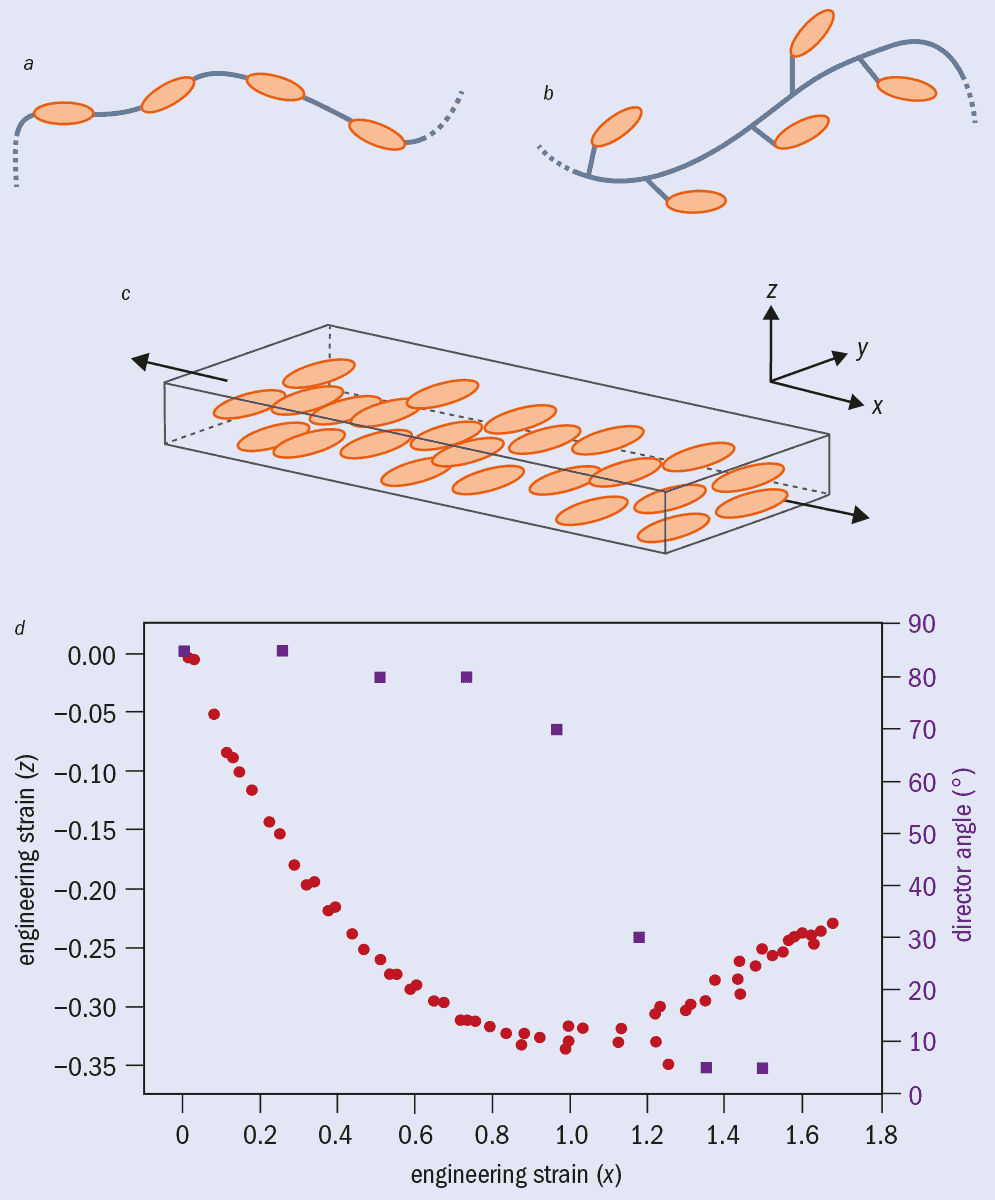
1 Auxetic behaviour in liquid-crystal elastomers Liquid crystals found in mobile-phone screens or TVs usually consist of rod-like molecules that point in roughly the same direction, known as the “director”. However, liquid-crystal behaviour can also be obtained from long-chain polymers that have rod-like units strung along the backbone (a) or stuck out from the side (b). If the neighbouring chains are physically connected, you end up with a “liquid-crystal elastomer”, which has some unusual mechanical properties, as our group at the University of Leeds, UK, found when we strained a thin film of the material in the x direction (c). We discovered that its strain in the z direction (red dots in (d)) and associated change in thickness falls as expected before suddenly increasing again. At this threshold strain of 0.9, the angle (purple squares in (d)) between the director and the x-axis drops from 90° (i.e. perpendicular to the strain) to 0° (i.e. parallel to the strain).
Now although most liquid crystals – including those in displays – contain small molecules, it’s also possible to obtain liquid-crystalline behaviour from long-chain polymers that have small, rod-like units strung out along their backbone (figure 1a) or stuck out from the side (figure 1b). When these rods line up, the polymers act like liquid crystals. What’s more, if the rods on one polymer chain are physically connected (or “cross-linked”) to more than one chain, you end up with the kind of liquid-crystal elastomer (LCE) that Mistry was studying.
Combining the elasticity of an ordinary elastomer (like rubber) with the self-organization of a liquid crystal, these soft materials have some unusual anisotropic mechanical properties. But because there was no chemist on our Leeds team at the time for him to draw on, Mistry decided to develop an LCE that he could easily synthesize himself using a known synthetic pathway and commercially available monomers – a “physicist-friendly” LCE as he put it. Using techniques borrowed from the liquid-crystal display industry, Mistry was able to make highly uniform thin films of his materials, in which the orientation of the rods can be controlled over large areas.
Strange behaviour
Having developed his new LCE material, which had rods as side groups, Mistry and a group of technicians from Leeds started building a special piece of equipment for testing its mechanical properties. The equipment was designed so that it could fit onto the stage of a polarizing microscope – one of the tools-of-the-trade in liquid-crystal physics. Using the rig, Mistry was able to measure the angle of the director at a chosen point in the LCE, which indicates the amount of local liquid-crystalline order, and monitor how this changes as the strain is increased.
When he pulled the film in the x direction – perpendicular to the director, which pointed in the y direction (figure 1c) – nothing of note initially happened. The material simply stretched in a soft elastic fashion and the director remained about 90° to the stretching direction. However, once it was stretched beyond a threshold strain of 0.9, the director rapidly began to line up with the strain axis – in other words, the angle between the director and the stretching direction fell to 0°. By simultaneously measuring the dimensions of the LCE film, Mistry concluded that it was behaving as an auxetic material – it was getting thicker in the z direction, at 90° to the direction in which it was being stretched.
There were two possible explanations for this unexpected auxetic behaviour. The first, rather mundane, option was that the strain on the sample had simply lowered the material’s density, meaning that pores had formed in it as with all other ordinary auxetics. But when Mistry carried out further mechanical studies using cryo-scanning electron microscopy and atomic-force microscopy, it appeared that the volume – and hence density – remained unchanged, which meant that no nanometre-sized pores had formed.
That therefore left the other, more exciting, option, which was that the LCE’s auxetic behaviour was occurring at the molecular scale. Incredibly, Mistry had discovered a material that, when strained beyond a certain threshold value (0.9), thickened perpendicular to the direction in which it was being stretched without the formation of voids. Somehow the polymer was rearranging itself at a local molecular level to trigger auxetic behaviour (figure 1d).
What’s more, Mistry soon noticed that the threshold strain dictating the onset of auxetic behaviour coincided with what appeared to be an order parameter of zero – and potentially even less than zero. An order parameter less than zero might seem odd, but in this case it means that the rod-like units are randomly oriented in the x–y plane of the material, while the director itself points in the z-direction, out of the plane.
Further insights have been uncovered by Thomas Raistrick, one of my current PhD students. His quantitative Raman-scattering measurements have shown that the uniaxial order of the material (meaning it has only one axis of anisotropy) falls to zero as the material is stretched. But just before the threshold strain, biaxial behaviour emerges (meaning the material now has two axes of anisotropy). As the strain increases further, the material begins to return to a uniaxial state. We need to do more work, but it’s clear that a complex interchange of order and symmetry causes the auxetic response, with further insights hopefully emerging soon.
Applications ahead
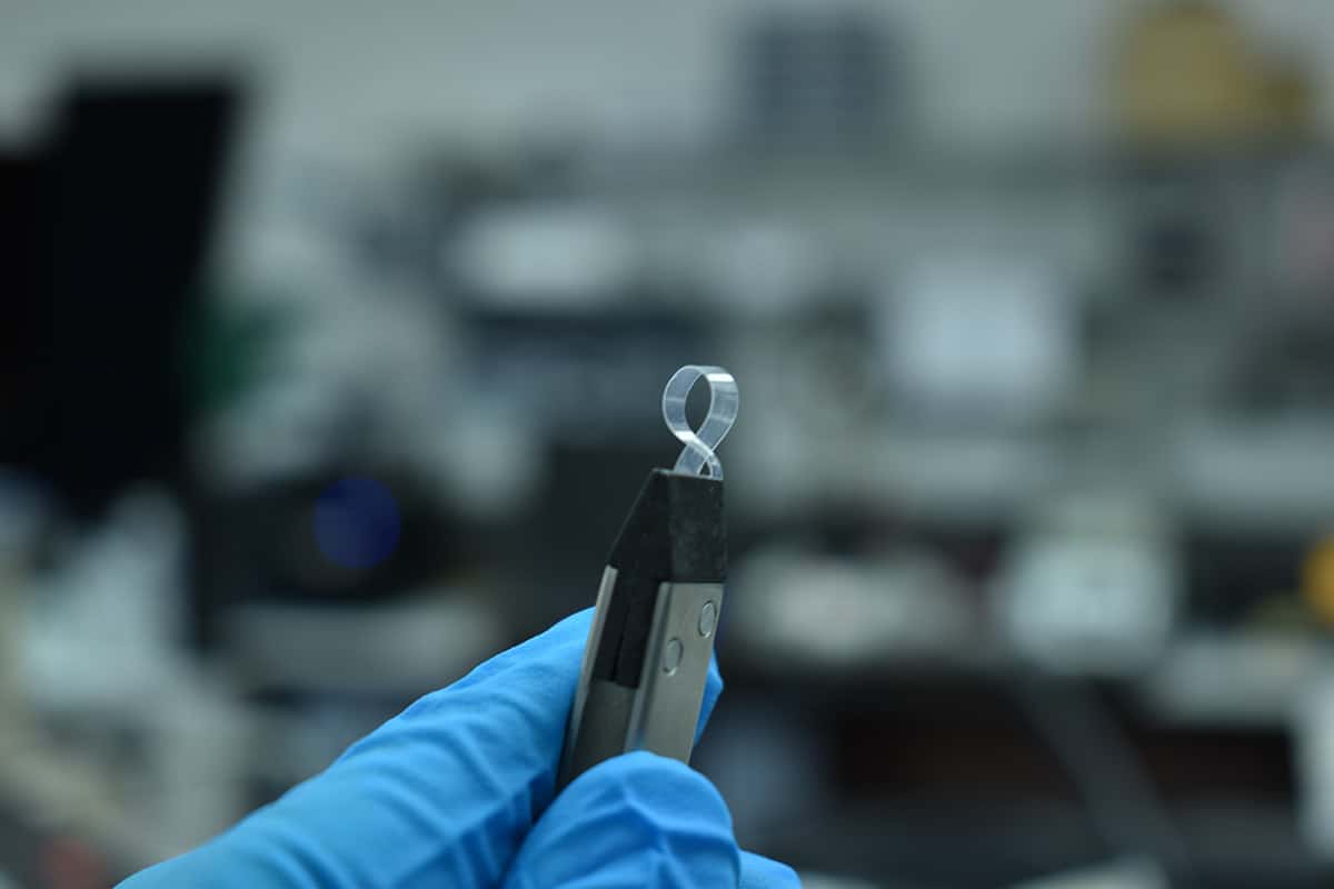
What’s so interesting about this LCE’s auxetic behaviour is that it occurs at the molecular scale rather than relying on the behaviour of macroscopic pores found in other “first-generation” synthetic auxetic materials. It therefore does not become inherently weaker when stretched, which means it could be used, say, as body armour, where you need a material that is likely to come under a lot of impact. The material would then act as a shock absorber – thickening in response to the force, rather than becoming thinner like a standard positive-Poisson-ratio material.
Clear benefits This transparent liquid-crystal elastomer displays auxetic behaviour when stretched – not because voids form inside it (as with ordinary auxetics) but because the structure reorganizes internally at a molecular level. (Courtesy: Ethan Jull, University of Leeds)
These transparent molecular auxetics could also be useful in the automotive industry to protect car windows, which usually have several layers of glass separated by layers of polymer. When hit, the induced strain makes all the layers shrink and so can become unstuck or “delaminate”. But if you had an auxetic material with a negative Poisson ratio, it would – if hit – expand against each layer of glass and stop any delamination from occurring. Molecular auxetics could also, for the same reason, be used in solar cells, which usually come with a 25-year warranty and need to stay robust for long periods.
Our team at Leeds, including Mariam Hussain, Richard Mandle, Ethan Jull, Keith Rollins and Peter Hine, is currently exploring these protection and delamination prevention applications. We believe that molecular auxetic LCEs could be game-changers – not just because they’re robust, transparent and thicken when stretched, but also because we can effectively tune these materials at the molecular level simply by adjusting their chemical make-up.
The author thanks Ethan Jull of the University of Leeds for the original draft of this article
Roger Penrose is one of the recipients of this year’s Nobel Prize for Physics. The British mathematical physicist was honoured for his discovery that black-hole formation is a robust prediction of the general theory of relativity.
In this interview with Physics World’s Tushna Commissariat, recorded in 2015, Penrose looks back to the early years of his career as a PhD student at the University of Cambridge. Penrose describes how he was inspired by courses given by eminent physicists including Paul Dirac and Hermann Bondi. But his career-long interest in black holes was triggered by attending a lecture by David Finkelstein on the nature of event horizons and the concept of a singularity.
Speaking at the “Celebrating 100 Years of General Relativity” event at Queen Mary University of London, Penrose also looks to the future of his field. He believes that in the long-standing quest to unify the theories of gravity and quantum mechanics, it is quantum theory that must be modified significantly beyond its current form. The (now) Nobel laureate refers to this process as the “gravitization of quantum mechanics”.


 Thibault Brulé is Raman application scientist at HORIBA France, working in the Demonstration Centre at the HORIBA Laboratory in Palaiseau. He is responsible for providing Raman spectroscopy applications support to key customers from various industries, as well as contributing to HORIBA’s application strategies. Prior to joining HORIBA in 2017, he conducted research on proteins in blood characterization based on dynamic surface enhanced Raman spectroscopy. He then applied this technique to cell-secretion monitoring. Thibault holds a MSc from the University of Technologies of Troyes, completed his PhD at the University of Burgundy and followed on with a postdoc fellowship at the University of Montreal.
 Agnès Tempez is application scientist at HORIBA France, working in the Nanoscopy group, connected to the Demonstration Centre at the HORIBA Laboratory in Palaiseau. She is responsible for providing applications support to key customers involved in nanoscopy and TOF-related research projects. Prior to joining HORIBA in 2006 as project manager, she worked as a research scientist at Ionwerks, Inc. in Houston, Texas, to develop time-of-flight mass spectrometry instrumentation for materials characterization and MALDI/ion mobility coupling for complex biological samples. Agnès holds a PhD in analytical chemistry from the University of Houston, Texas. She is the author of nine patents, one book chapter and more than 75 articles in peer-reviewed journals.