Topological effect creates unidirectional photonic device

A photonic device that radiates light only in one direction has been created by researchers in China and the US. Chao Peng, Marin Soljačić and colleagues at Peking University, the Massachusetts Institute of Technology and the University of Pennsylvania created their device by carefully tailoring the shape of a set of etched silica bars – thereby using topology to modify a curious effect that was predicted 90 years ago. The optical device could have multiple applications in optoelectronics.

A key challenge in creating optical circuits is that light will happily travel in both directions through optical devices – which causes unwanted effects. Current solutions such integrating a mirror to reflect light travelling in the wrong direction tend to be bulky, inefficient or difficult to fabricate. Now, researchers in China and the US have put a topological twist on an effect first proposed in 1929 and created a photonic crystal that rediates light in only one direction.

In 1929, John von Neumann and Eugene Wigner discovered that some solutions of the Schrödinger equation for an electron in a potential well involved bound states that nevertheless had enough energy to escape the well. Creating experimental systems that exhibit these “bound states in the continuum” (BICs) was not possible at the time so they remained a mathematical curiosity for several decades. Beginning in the 1970s, researchers realized that the same physics applied beyond quantum mechanics and more broadly to systems of waves. Since then, BICs have been observed in light, sound and water waves as well as surface waves in graphene.

A perfect mirror

In 2013, a team led by Soljačić used BICs to produce a new type of perfect mirror that could trap and reflect light without ever absorbing it. In 2017, Boubacar Kanté at the University of California, San Diego and colleagues extended the concept from controlling the trapping of light to tailoring its emission. They produced an optical “supercavity” from a square lattice structure of indium gallium arsenide phosphide. When pumped at optical frequencies, their structure supported a standing wave at around 1550 nm (the wavelength most commonly used in telecommunications). This was used to create a very narrow linewidth laser that could prove useful in optoelectronics.  However, the emission is spatially symmetric: just as many photons are radiated downwards from the lattice as upwards.

In the latest research research, Soljačić and colleagues in the US and China developed a neat trick to produce an device that sends radiation in only one direction. The team fabricated a periodic array of 500 nm deep and 200 nm wide silicon bars approximately 1 micron apart on a silica substrate. If the bars had been created perpendicular to the substrate, simulations suggested the system would behave as a BIC when excited with 1550 nm light. Instead, however, the researchers tilted the bars slightly, disrupting the BIC and allowing radiation to leak out.

Topological considerations meant that radiation radiated upwards had to have the opposite polarization to radiation emitted downwards. When the bars had been tilted far enough, any radiation radiated downwards would have to be both left-circularly-polarized and right-circularly-polarized at the same time. As no radiation could ever satisfy this constraint, radiation should not be emitted downwards – and least for a perfectly constructed device. The actual device sent thousands of times more optical power upwards than downwards.

“Beautiful work”

Soljačić and colleagues were unavailable for comment, but Kanté – now at the University of California, Berkeley – describes the research as “beautiful work”. “This is probably the highest contrast I have ever seen in a passive structure,” he says. “Normally the ratio is one to two, three or four.” He believes the most interesting aspect is the underlying theory the researchers use to break spatial symmetry and show how radiation can be cancelled in one direction.

He adds a note of caution, however: “Unidirectional does not mean non-reciprocal: even if it only sends signals out in one direction it will still receive them [from both directions],” he says. “To avoid interference this antenna would still require an isolator.” This could have its own advantages, however: “Sometimes you want to be able to couple light efficiently into an optoelectronic chip or back out of it using something called a grating coupler,” he explains. “It could be very useful for that.”

The research described in Nature.

Got the lockdown blues? Take this trivia quiz on astronomy and space

1 What is another name for Tardigrades – the tiny creatures left on the Moon when Israel’s Beresheet craft crashed into the lunar surface in 2019? A Water bears B Water dragons C Water flies D Water horses

2 What object left on the Moon by Apollo astronauts do some scientists think should be retrieved by a future lunar mission? A Alan Shepard’s golf ball B Buzz Aldrin’s bag of faeces C Harrison Schmitt’s rock hammer D Gene Cernan’s lunar rover

3 Who or what were Harriot, Wangshu, Abol and Umbäässa? A Comets B Exoplanets C Craters on Mars D Presidents of the International Astronomical Union

4 What name was given to the two ultra-high energy neutrinos detected in 2014 by the IceCube observatory at the South Pole? A Bill and Ben B Bert and Ernie C Tom and Jerry D Batman and Robin

5 How many of the astronauts on the Apollo 11 mission were quarantined when they returned to Earth? A None B One C Two D Three

6 What topping featured on a Pizza Hut pizza delivered to the International Space Station in 2001? A Anchovies B Mushrooms C Pepperoni D Salami

7 What was the error in the size of the perimeter of the primary mirror on the Hubble Space Telescope after launch in 1990? A 2.2 nanometres B 2.2 microns C 2.2 millimetres D 2.2 centimetres

8 What society did astronomers Mary Blagg, Ella Church, Grace Cook and Fiammetta Wilson become the first female elected fellows of in 1916? A Royal Society B American Astronomical Society C Royal Astronomical Society D Astronomical Society of the Pacific

9 What did NASA recently name its Mars rover to? A Persistance B Perserverance C Persuasion D Perscipacity

10 What kind of lettuce was recently grown on the International Space Station? A Iceberg B Red romaine C Lollo rosso D Frisée

Want to know the answers? We’ll reveal all next week on Friday 1 May.

Update: Answers below the sponsor’s message.

UHV Design logo

Sponsored by UHV Design Ltd, specialists in the design, manufacture and supply of high-quality, low-maintenance, manipulation and heating solutions for thin film deposition, surface-analysis instrumentation and particle-accelerator diagnostics. Visit uhvdesign.com to learn more.

Answers: 1 A    2 B    3 B    4 B   5 D    6 C    7 B   8 C   9 B   10 B

Get Precise Tribology Data Through Surface Profilometry

View on demand

This webinar provides an overview of how advanced optical profilometry can contribute to successful tribology tests, and allows one to extract critical data such as wear rate, life time, time to failure and volume removal rates. First, white light interferometry based optical profiling will be introduced. Next, we will present how this method can be applied across a wide range of tribological tests from micron-indentations to high-speed reciprocating tests via scratching and pin-on-disk approaches.  A live practical session will conclude this webinar.

Presenters:


Dr Samuel Lesko
Senior Application Development Manager

Dr Michel Fajfrowski
Application Manager

Combining Atomic Force Microscopy with Optical Techniques

View on demand

This webinar will focus on how AFM can be integrated into optical techniques. You will learn concepts from basic sample observation up to single molecule advanced super-resolution inverted optical microscopy simultaneous to AFM. The webinar will also elucidate how tip-enhancement techniques can provide more comprehensive data sets. We will also focus on how high-NA upright optical techniques can be used with AFM on opaque samples or substrates.

Presenters:
Dr Florien Kumpfe
JPK BioAFM Application Scientist


Carmen Pettersson
Senior Manager Product Marketing Manager

NanoDMA III for Polymers: Primer and Applications

View on demand

This webinar will start with some basic nanoindentation theory and focus on its shortcomings with regards to the unique mechanical characteristics of polymers, particularly their strong time-dependence. To overcome this shortcoming, a nanoscale compliment of Dynamic Mechanical Analysis, Bruker’s nanoDMA III presented. This simple method measures both storage (E’) and loss (E’’) modulus of polymeric materials in a meaningful way.

Having the basics in hand, the nanoDMA III technique can then be applied to increasingly difficult (and often more rewarding) measurements:
• Combining effects of time and temperature for something easy; a thermoplastic, then something more difficult; a liquid silicone.
• Advantages of small-scale testing of bulk polymers over a wide variation in humidity conditions.
• Measuring temperature effects on adhesion, E’ & E’’, and uniformity of coating for pressure sensitive adhesives.

Presenters:

Dr Douglas Stauffer
Senior Manager NI Applications


Dr Rhys Jones
Nanoindentation Product Sales Specialis

Hubble’s best shots: eXtreme Deep Field

Thanks to the finite speed of light, the deeper we look into space, the further back in time we go. But how far back can we see? Hubble’s eXtreme Deep Field answers that question with our deepest-ever view of the universe: some of those faint patches of light in it are galaxies dating back more than 13.2 billion years.

This window into the past gives cosmologists insight into how the earliest galaxies – more than 5000 of which fill the view in this tiny patch of sky – grew as they emerge from a truly ancient era known as the Dark Ages. But the galaxies of the era visible in this image are already a few hundred million years old. To witness the birth of the very first stars and galaxies, we will need a telescope beyond even the capabilities of Hubble.

Fortunately, we should have one soon: the long-delayed James Webb Space Telescope (JWST), currently scheduled for launch in 2021. Designed to observe the universe at infrared wavelengths, it won’t be a true successor to Hubble, but it should prove just as profound in advancing our knowledge of the cosmos as Hubble has been – and continues to be.

Stereotactic ablative radiation to metastases slows prostate cancer progression

Stereotactic ablative radiotherapy

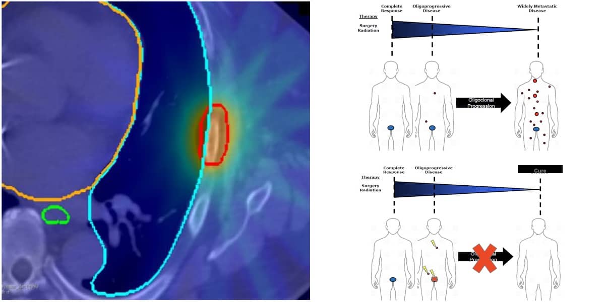
Stereotactic ablative radiotherapy (SABR) is a popular method for treating small, inoperable tumours in various anatomical sites. This type of radiotherapy delivers highly focused, intense radiation doses in few treatment sessions, which increases the radiation’s cell-killing effectiveness. A phase II study conducted by researchers from the Johns Hopkins Sidney Kimmel Cancer Center has now shown that SABR can slow disease progression in prostate cancer patients with up to three metastases (JAMA Oncol. 10.1001/jamaoncol.2020.0147).

Prostate cancer is the second most common cancer in men worldwide and the most common in the USA and many European countries. Once the tumour has metastasized, the disease is incurable, though treatment options exist that can slow its progression. One standard treatment for men with hormone-sensitive metastatic prostate cancer is a type of hormone therapy called androgen deprivation therapy (ADT). However, ADT can have side effects such as impotence or loss of bone and muscle density. Many men therefore prefer to delay this treatment for as long as possible.

SABR as an alternative to early hormone therapy

Recently, SABR has been gaining interest as a treatment option for cancers in the early metastatic (oligometastatic) stage, where patients have few, localized metastases. The results of the ORIOLE (Observation versus Stereotactic Ablative Radiotherapy for Oligometastatic Prostate Cancer) phase II randomized controlled trial suggest that treating prostate cancer oligometastases with SABR early on could be a strategy to delay the need for ADT and its harsh side effects.

The trial included 54 men with recurrent hormone-sensitive prostate cancer, and between one and three metastases, who were randomized to receive either SABR or observation only.

Ryan Phillips and Phuoc Tran

The researchers, led by Phuoc Tran of the Johns Hopkins University School of Medicine, report that of 36 patients treated with SABR only, seven (19%) suffered disease progression after six months, while 11 of 18 (61%) in the observation-only group did. Tran and colleagues further report no severe side effects in the SABR trial arm and no significant difference in patient-reported quality-of-life when compared with the observation-only arm.

Triggering the immune system

In addition to showing SABR’s safety and effectiveness for treating these patients, the ORIOLE trial results also hint at an underlying mechanism. The researchers detected an expanded population of T cells in the blood of patients treated with SABR compared with observation-only patients. This suggests that the treatment may have stimulated a body-wide immune response towards the tumours.

“It has been a longstanding question, especially important now in the era of immunotherapy, whether any type of radiation, and SABR specifically, can stimulate the immune system,” Tran said in a recent press release. “Our trial offers the best data to date to suggest that SABR can cause a systemic immune response.”

Finally, the team found that the patients could be divided into low-risk and high-risk groups based on specific tumour gene mutations. They found that SABR was especially effective at slowing disease progression in the low-risk group, indicating that tumour DNA mutation profiles might predict how well a patient responds to SABR.

While these results point to exciting possibilities for new combined treatments and patient risk stratification, Tran and colleagues caution that further studies are needed to validate these insights. Currently, the team is focusing its efforts on further investigating disease-slowing treatments for metastatic cancers. For example, in an ongoing trial called RAVENS, they examine the effect of combining SABR with radium-223 to combat bone metastases.

Automated alignment: a game-changer in quantum photonics

The future of photonics is taking shape along two converging coordinates as on-chip optical integration meets next-generation quantum technologies that exploit the exotic properties of quantum mechanics – entanglement, tunnelling, superposition and the like. The end-game: integrated quantum photonic devices, produced at scale, to controllably manipulate the quantum states of optical materials, opening the way to practical applications like quantum computing, quantum communications, quantum metrology and quantum imaging.

To make that quantum vision a reality – initially in an R&D context, though ultimately in terms of volume production and manufacturability – the German precision motion specialist PI (Physik Instrumente) has addressed a vexing, costly and long-term bottleneck in the testing, characterization and manufacturing of photonic devices down to the atomic scale.

Here Scott Jordan, head of the photonics market segment for PI, tells Physics World how the company’s Fast Multichannel Photonics Alignment (FMPA) technology – a set of firmware-level commands built into the vendor’s digital nanopositioning controllers, intelligent microrobots and stage controllers – can help developers to automate the optical alignment, test and assembly of quantum photonics devices while driving down production costs.

Why is automated active alignment – the foundation of FMPA – so important for the assembly of photonic devices?

There are growing requirements to align and position multiple optical components – for example, the lenses in smartphone cameras or the CCD chip itself – with nanoscale accuracy and economic efficiency. In integrated silicon photonics and next-generation quantum photonics, a multitude of tiny active and passive optical devices must be aligned for testing and packaging, starting at the wafer level. The common theme is multiple channels, multiple elements, multiple interacting inputs and outputs, multiple degrees of freedom – all need to be aligned and optimized multiple times throughout the manufacturing process.

If this is the problem, FMPA technology is part of the answer. Put simply, aligning the inputs and outputs of integrated photonic devices at industrial pace requires parallel optimization and nanoscale accuracy – not least in the coupling of on-chip waveguides with optical fibres. As we move into the quantum photonics realm, with its more complex production and test requirements, this parallelism will become increasingly critical to the process economics.

It sounds like the parallelism offered by FMPA has been a game-changer in photonics R&D and manufacturing?

FMPA is a huge advance over previous automated alignment technologies. Optical alignment is the single biggest cost/time sink in the testing and packaging of integrated photonic devices. In the short waveguides, typically millimetre-scale or less as increasingly deployed in silicon photonic devices, the input and output couplings can steer each other – so as one side is optimized, the other shifts slightly and needs reoptimization. In the past, this necessitated a time-consuming, serial sequence of back-and-forth adjustments of the input, then the output, repeating and iterating towards a global consensus alignment.

Similarly, when optimizing an angle, the transverse alignment would be impacted and would conventionally need to be reoptimized, again in a time-consuming serial loop. With FMPA, these interacting alignments can be optimized simultaneously to deliver a global consensus alignment, often in one go. In many cases, tracking and continuous optimization of all the alignments is also possible, allowing compensation of drift, curing stresses, and so on.

At a fundamental level, how do PI’s intelligent microrobots deliver optical alignment?

Scott Jordan

At PI we make precision motion and nanopositioning technologies. Over the past four years, we have implemented a new generation of algorithms in the controllers for this equipment. These algorithms intelligently seek the optimum of a given optical figure of merit versus position. There are two types of alignment process: area scans to localize the main peak for a given parameter (e.g. optical power, modulation transfer function or modal purity) within a defined region, while parallel gradient searches efficiently optimize one or more such couplings at once – and optionally track them to mitigate drift processes and positional disturbances caused by temperature changes. In the case of a coupling between an on-chip waveguide and an optical fibre, for example, the manufacturer typically wants the alignment to minimize the light loss going from one element to another.

How have PI’s customers responded to FMPA technology?

The commercial launch of our parallel alignment technology was well timed. When we introduced FMPA four years ago, we found a niche with research and industry customers searching for faster optical alignment solutions to improve their production and test economics. A big driver is silicon photonic devices with arrayed-waveguide inputs and outputs – multiple optical channels that must be aligned simultaneously with optical fibres or other elements. To meet that need, we now have leading industrial players in silicon photonics – the likes of FormFactor Inc in the US, MPI in Taiwan and Tegema in the Netherlands – building high-throughput test and assembly equipment – photonic wafer probers and packaging-automation tools, respectively – based on our microrobots, positioning stages and advanced controls technology.

So FMPA is already being exploited to support early-stage device R&D in quantum photonics?

Absolutely. FMPA is at the heart of leading-edge photonic wafer probers that are being deployed by industry for testing of prototype quantum photonic devices – as well as optimizing the fabrication processes for such quantum devices. The probers are used to test the electronic and optical functionality of each photonic device on the wafer, so that the developer knows which devices are worth packaging. The same functional elements are routinely deployed on the benchtop level as well.

Is FMPA also being used by academic researchers working on quantum photonics?

We work with many pioneering academic customers to support development of next-generation quantum photonic devices. A case in point is a team led by Vlad Shalaev at Purdue University (West Lafayette, IN), who are using our FMPA systems to map, track and characterize novel single-photon quantum emitters that could prove fundamental to photonic implementations in quantum computing.

Essentially, the Purdue team has demonstrated high-brightness, single-photon quantum sources operating at room temperature – creating streams of fully randomized photons from atomic defects in nanoscale diamond films. To make use of the photons created by these defects, however, it is first necessary to collect them, guide them down an optical fibre, and measure them using a photon counter (typically tens of thousands of photons per millisecond).

With this in mind, we helped them build an open-source FMPA workstation comprising a very-high-precision xy positioning stage with an aperture in the middle – a set-up that is used to scan and lock onto the atomic-scale emitters so that they can be characterized. The workstation software took only eight hours to build from scratch, largely because all the functionality is incorporated into our motion controllers. All in, a neat example of PI’s alignment technologies being put to work in a fundamental research context that has demonstrated some world-leading results.

Neutrinos provide insight into why matter dominates the universe, celebrating the Hubble Space Telescope’s 30th birthday

One of the enduring mysteries of physics is why the universe appears to contain much more matter than antimatter. An important clue has just been unearthed by the T2K experiment in Japan, which found a difference in what happens to muon neutrinos and antineutrinos as they travel through nearly 300 km of solid rock. In this episode the Durham University particle physicist Silvia Pascoli discusses the implications of the T2K result with Physics World’s Hamish Johnston.

Tomorrow (24 April) is the 30th anniversary of the NASA’s Hubble Space Telescope and the astronomy writer Keith Cooper has done a series of blogs for Physics World describing his favourite images. In the podcast he joins Margaret Harris for a lively chat about all things Hubble. Their wide-ranging discussion begins with how the telescope was saved from ruin in its early days and ends by pondering the mission’s future.

2D materials can enable futuristic optoelectronics technologies

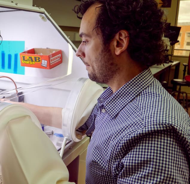
Andrés Castellanos-Gómez is a materials researcher who combines tradition with the cutting edge. His group at the Materials Science Institute of Madrid is interested in complex oxides, which are grown epitaxially on the surface of crystals before being isolated from their substrate by etching. Alongside this long established method, the team deploys techniques from the emerging field of 2D materials to create 2D heterostructures held together by Van der Waals forces.

Andrés Castellanos-Gómez

Employing this combined approach, Castellanos-Gómez’s group creates prototype “straintronics” devices – tuneable electronic components whose properties change upon the application of strain. One example is the concept of a camera that could be switched from detecting visible light to infrared light simply by applying strain to the pixels within its sensor.

Castellanos-Gómez describes this research in this interview with Physics World, recorded recently before Spain’s lockdown began in March. He also explains how his team works with a network of other European research groups under the EU’s Graphene Flagship programme.

Find out more about the materials research taking place at the ICMM in this video profile we shared last week. Also take a look at the Physics World Nanotechnology Briefing, published in April 2020. This free-to-read collection celebrates how nanotechnology is playing an increasingly important role in applications as diverse as medicine, fire safety and quantum information.

Copyright © 2025 by IOP Publishing Ltd and individual contributors