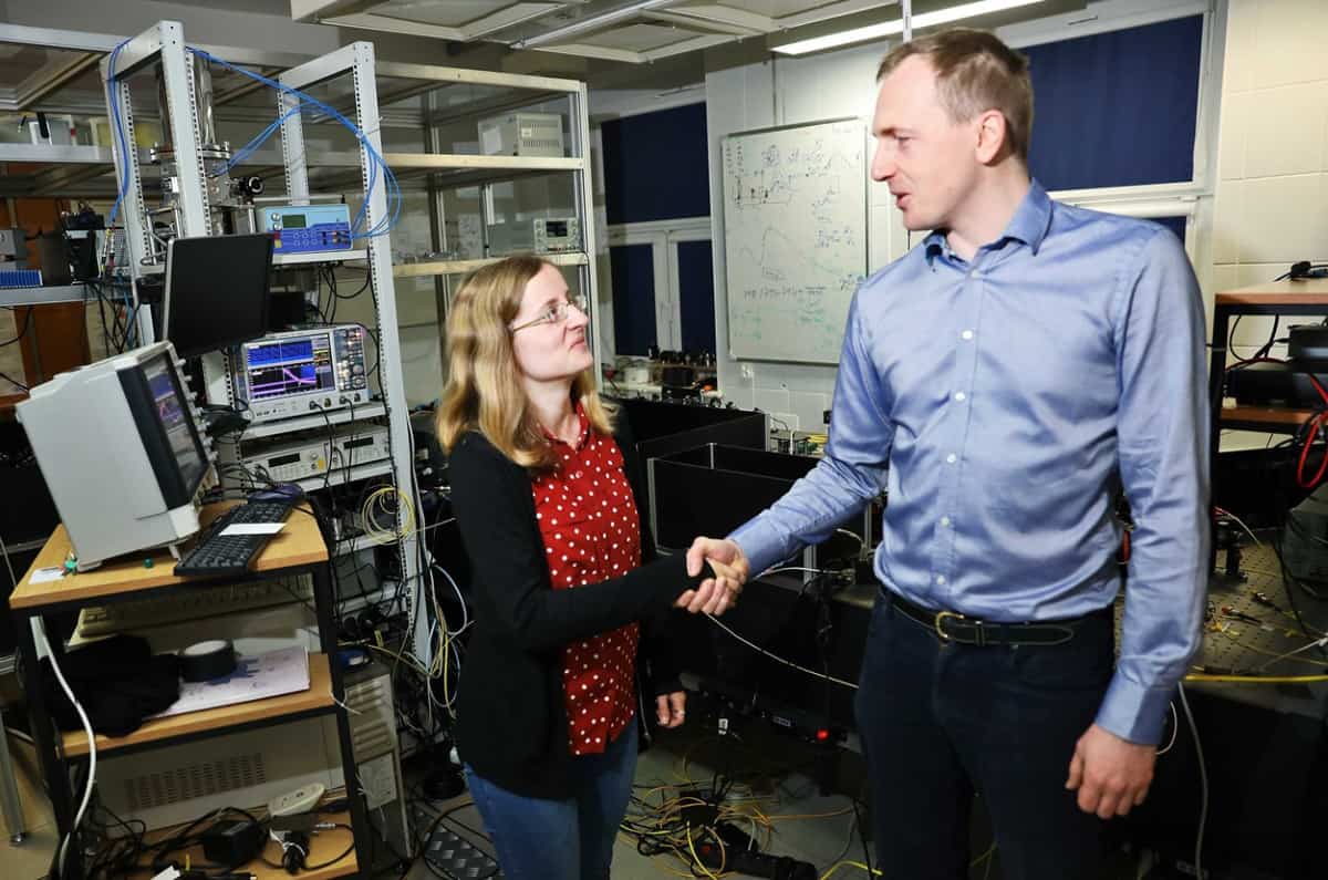
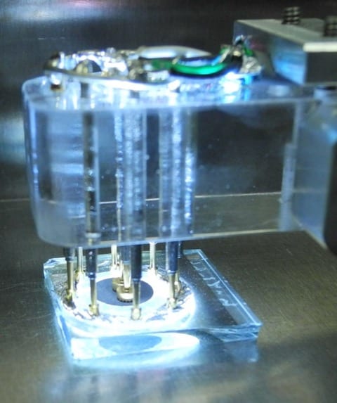
Researchers Sylwia Kolenderska and Piotr Kolenderski are using single-photon detectors to enhance OCT. (Courtesy: Andrzej Romański, Sylwia Kolenderska)
A novel detection method for optical coherence tomography (OCT) achieves high-quality imaging at low light intensity. The new OCT method was developed by a group of researchers from the University of Auckland in New Zealand and the Nicolaus Copernicus University in Poland. Borrowing ideas for their detection mechanism from quantum optics, they describe in Optics Letters how the method can produce comparable results to standard OCT systems at very low light intensity levels (around 10 pW).
OCT is a widely used medical imaging technique that can non-invasively obtain cross-sectional images of semi-translucent materials. It has applications in several medical disciplines, including ophthalmology, cardiology and dermatology, where its resolution allows visualization of microscopic details. It works by illuminating the tissue with broad-bandwidth visible or near-infrared light. This light is scattered and reflected by the biological media and then captured and assessed using a spectroscopic detector.
OCT can provide images of tissue morphology at 1 µm resolution and it is now a common part of routine eye exams, where an ophthalmologist may recommend the scan to inspect the retina’s distinctive layers and rule out glaucoma or retinal diseases.
In a clinical setting, OCT is limited by the allowed intensity levels. For example, the imposed safety levels for imaging the eye are 1.7 and 5 mW, at wavelengths of 800 and 1060 nm, respectively, constraints that can sometimes affect the fidelity of the obtained images. A team led by Sylwia Kolenderska bypassed this limitation by using a superconducting single-photon detector (SSPD) instead of the standard OCT detector – an idea inspired by quantum optics, where SSPDs are used to study various properties of single photons.
One photon at a time…
Leading the way towards high-fidelity low-power OCT systems, the team came up with the idea of using an SSPD while researching new OCT detection schemes. As these sensors can detect single photons, the proposed setup uses a much smaller amount of light than a standard OCT system. In fact, the required power is a few orders of magnitude smaller than clinically available counterparts.
To make the new detection scheme work, the team had to make a few changes to the original optical setup, which requires a way of discerning the different wavelengths of light being reflected from the imaged object. As they were now working in a single-photon detection regime, the researchers decided to couple the SSPD with a long (5 km) fibre spool that induces a wavelength-dependent time delay. In other words, different wavelengths of light will travel at different speeds down this fibre, enabling the SSPD to capture the light spectrum.
…yields high-quality images
The team tested the new OCT setup using a 1550 nm pulsed light source to image two objects: a stack of different types of glass and a slice of onion. The glass stack was made up of three layers: quartz (50 µm thick), sapphire (460 µm thick) and BK7 glass (500 µm thick), and it was used as a controlled test to understand how well the different layers can be discerned. The slice of onion was used as a biological sample. Both experiments resulted in good-quality images, comparable with images obtained by standard OCT systems, but using intensity levels five orders of magnitude lower.
The researchers point out that they observed artefacts in the reconstructed images. These are unwanted image features that, in this case, appear because the detection system is recording all types of interactions between photons inside the sample. Artefact removal algorithms can be used to clean up the images and are straightforward to use when the imaged object has a well-defined structure, such as the stack of glass. These artefacts become more problematic when dealing with biological samples, where the structure is highly heterogeneous and complicated.
Participants will learn how RadCalc’s 3D packages can improve accuracy, efficiency and safety in the QA process even if working from a remote location.
The webinar, presented by Dana Cooper, will help the audience to explore:
The workflow of the RadCalc 3D.
The commissioning process and analysis.
Types of plans for RadCalc in a challenging environment such as this pandemic.
Dana Cooper is a certified medical dosimetrist/technical sales representative with LifeLine Software, Inc, part of the LAP Group. She has more than 25 years of experience in radiation oncology, having held positions such as radiation therapist, dosimetrist and department manager. Dana joined LSI in 2016 and has been connecting radiation therapy departments with software that increases productivity and safety ever since.
Making waves Gray giving a talk at Humboldt State University’s Distinguished Alumni Speaker Series in 2019. (Courtesy: Humboldt State University, Kellie Brown)
What sparked your initial interest in physics?
I was interested in science from a young age thanks to my dad, who was an engineer. He would do a lot of projects at home – work on the car and build things in the garage – so I always thought that was interesting. My dad was one of my first role models, but there were also some teachers who were a real inspiration. I enjoy a lot of TV and film too. When I was in high school there was a popular US TV show MacGyver. I religiously watched that every week, and I wanted to be an Indigenous MacGyver.
Tell me a bit about your educational background, and what your degree focused on.
I grew up in southern California, and went to the local California State University (CSU), which was in San Bernardino. I didn’t know what I wanted to study yet, so I was undeclared for the first year. I then wanted a change of scenery, so in my second year I applied for the furthest away CSU campus, which was Humboldt State, on the coast of northern California, just south of the Oregon border. That’s where I finished my undergrad, and I decided upon studying physics. I’m not going to lie, it was hard – the courses were tough, and being away from home was difficult. What helped me was finding a new family there, thanks to the Indian Natural Resources Science and Engineering Program (INRSEP). Right when I was homesick, crying in my dorm room and wanting to leave, that’s when I found INRSEP – it kept me going, and helped me stay at Humboldt State. I did two science-related internships towards the end of my degree, which were very valuable. One of them was at a blood lab at the University of California, San Francisco. I soon found out that that wasn’t for me. I once accidentally evacuated the lab by spilling something that smelled horrible!
Years later, I received my bachelor’s of science (BS) degree in physics, and because there was so much maths involved, I also received a BS in applied mathematics.
So you began working at LIGO once you graduated – what was your first role there?
Yes, it was my first job after undergrad. I took a few months’ break to look after my younger sisters while my mom did research overseas. I was applying for jobs, and spotted an ad in the LA Times – it was for a Caltech job, up in Washington State. The opportunity to move again was what caught my eye most, because I didn’t know anything about LIGO back then. But I applied anyway, and started in March 1998. Both of the LIGO observatories – at Hanford, and Livingston – had opened for operations the previous year. The instruments were at a point where the teams were getting ready to install and build the initial LIGO detectors.
The detector has many subsystems, and my team worked on the seismic isolation system. We’re the ones who installed the big optical tables that isolate the mirrors from any ground motion, so we have the biggest parts that were installed into the vacuum system. Once it was built, we learned what it meant to be an operator for a gravitational-wave detector – how to sit in the “driver’s seat” of the detector, operate it and eventually keep it running for data collection.
What was it like for you during the early years of the experiment, when no detections were made? Were you ever temped to leave?
When I first joined LIGO, I thought like most other people do about their first jobs: “I’ll be here for my resume for maybe five years, then move on to something different.” But a few things made me stay. One of the big things is that this job is never boring, because we get to do a lot of different things. I also love living in the north-west – we’re surrounded by beautiful countryside, so I do a lot of hiking.
From 2002 to 2010 we collected data with the initial LIGO detectors, and no detections were made. Operations for iLIGO ended in 2010, and we spent the next five years removing the majority of the iLIGO equipment from the vacuum system and installing advanced LIGO (aLIGO), before getting it into an operational state. aLIGO began taking data in late 2015.But as far as the big picture, I didn’t really have that until we started building aLIGO. Even then, I still didn’t think we would ever make a detection, because we went eight years with nothing.
One day while on a hike, I asked my roommate how likely he thought it was that aLIGO would actually make a detection. This was in summer 2011, and without skipping a beat, he told me, “We’re going to make detections”, before going into the detection rates. That’s when I first thought it was a possibility. And then we actually made the first detection on 14 September 2015. As soon as that happened, it changed our lives in so many ways.
Since then, aLIGO has made many observations. I don’t want to say it’s been boring or normal, but especially with the latest observational run (03), we have roughly one detection a week. Its become the new normal and that is such a good thing to be able to say. We are also working on upgrading the detectors all the time. But every time I get a message on my phone about a new detection, it’s still something I still get excited about.
What has been your experience as an Indigenous physicist in the US?
My tribe is Blackfoot, and I’m a member of the Siksika Nation from southern Alberta, Canada. Humboldt State is a small university, and I don’t know if there have been other Indigenous undergrads or Indigenous students from the physics department – there might have been in the last couple of years. But for sure when I was there, there weren’t any. Being alone was difficult, especially combined with the tough courses. It would’ve been nice to have role models who are like me. There was sometimes one other Indigenous physicist who I would see at national conferences. That’s definitely changing, but it’s still a pretty small number.
As far as work, the LIGO Scientific Collaboration (LSC) has around 1000–1200 people, and for the most part I was the only Indigenous person. In 2015, before the detection, an Indigenous grad student (Ron Tso, Navajo Nation) started at Caltech and joined the LSC. As soon as I heard, I contacted him, just to let him know that there’s another native person in the project. We’ve met a few times and given a few talks together, and it’s been really cool to have him be part of the team. I’ve since learned there are two other awesome Indigenous physicists in the LSC: Brittany Kamai (Caltech) and Mario Diaz (University of Texas at Rio Grande Valley).
There’s really not many Indigenous people in physics, and because of that I get a lot of requests for speaking engagements. Whenever there’s a chance for me to speak to Indigenous youth, or any other underrepresented groups, those are the ones that I prioritize. For example, earlier this year I spoke at the 2020 conferenceof the American Physical Society’s National Mentoring Community – which offers support to African American, Hispanic American and Native American students. This event sounded amazing, and I was honoured to have the opportunity to share my story and inspire other underrepresented people in physics. I also attend a few other national conferences such as the Society for the Advancement of Chicanos and Native Americans in Science and the American Indian Science and Engineering Society. So I’ve been able to network and meet other underrepresented people in the sciences.
Beyond your work at LIGO, you do a lot of science communication. Is this something you wanted to do from the start, or did you feel like you had to?
When I joined LIGO in 1998, I was fresh out of college. I just wanted to do my job building the machine, but I was asked by the head of the observatory to do some outreach work. He encouraged me to give talks, but I was shy and newly graduated – I had no idea about giving presentations or talks, and I really didn’t want to do it. So I was a reluctant science communicator at the start. But with lots of practice over the years and also LIGO’s first detection, everything changed – we had a huge story to tell.
I’m also aware that I do have a responsibility doing outreach activities with underrepresented groups. But it can be tough to do that as well as your day job and have a personal life as well. I get a lot of requests, and have to turn some down. I’m still learning how to sometimes say no. But most of the time, if it’s an underrepresented community, I will always say yes.
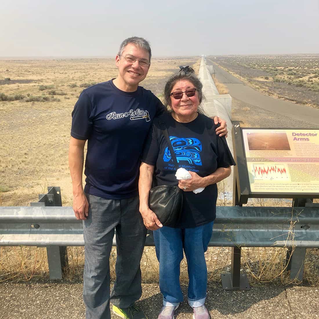
Family ties Gray with his mother, Sharon Yellowfly, at LIGO Hanford in 2017. The pair worked together to translate LIGO literature into Blackfoot. (Courtesy: Russell Barber)
You also had a special project, working with your mother to translate some of the LIGO press releases into Blackfoot. Tell me a bit about that.
It all came about a few weeks before we announced the first detection, in February 2016. We wanted to share this discovery with the world, so we wanted to get our press release translated into as many languages as possible. I asked for permission to translate it into Blackfoot. This would mean sharing the news of the discovery with someone outside of the collaboration – my mom. Thankfully my fellow collaborators thought it was a great idea, and I had permission within an hour.
My mom was so surprised and overwhelmed by the request, and she had only two weeks to work on it. She had a dictionary of Blackfoot words that she’s been putting together since she was in her 20s, so she used that along with tapes that she recorded of her parents, as well as reaching out to other family up north. Two weeks later, her translation was ready and went live with all the other 16 or 17 translations. She’s done five press release translations now. For the most recent discoveries made this year, she translated the technical science summaries. I’m very proud of the work we’ve done together.
What’s your advice for today’s students?
Don’t be intimidated by the job. When you start a new role, you are hopefully in a place that has good management – you should be able to read documentation, be mentored, and be taught how to do the work, to be able to succeed. It’s also really important to have a personal life, and give yourself time to recharge at the end of the day. Take vacations, have hobbies and do things that keep your sanity. Sometimes work can be stressful and hard, and you could get burned out if you don’t take care of these other aspects of your life.
Corey Grayworks at the NSF-funded LIGO Scientific Collaboration, part of the land-based gravitational-wave detector network including Virgo and KAGRA
Ever since Henry Ford launched the Model T in 1908 as the first truly mass-market car, the internal combustion engine has ruled the roads. The problem is that cars, vans and lorries powered by petrol and diesel have simply become too successful. Transport now accounts for almost a third of all greenhouse-gas emissions across Europe, some 90% of which is spewed out by road traffic. And the health risks posed by the particulates emitted by fossil-fuel engines have prompted many cities to ban or restrict the worst offenders from central districts.
It’s no surprise, then, that the future looks electric. Prices are falling, batteries are improving, and more people are opting to buy plug-in hybrid or fully electric vehicles for the first time. The International Energy Association (IEA) reported a 63% increase in the global fleet of electric cars in 2018, while in the UK battery-powered models accounted for a record-breaking 13% of all new car sales in March this year – even though the overall market for new cars shrunk due to the coronavirus pandemic.
Indeed, current projections suggest that savvy buyers will make a large-scale shift to electric vehicles within the next five years. The initial outlay may still be higher, but more affordable models are now reaching the market and government incentives can often bring down the price differential. Electric cars are also significantly cheaper to run: the cost of electricity is about a third that of fossil fuels to travel the same distance, while fewer moving parts in all-electric models can reduce maintenance bills by up to 60%. Throw in the reduced resale value for gas guzzlers, more than a dozen countries having already set dates for when they will ban the sales of new petrol and diesel cars, and the smart money will go electric.
Some countries are already ahead of the curve. Norway, for example, offers generous tax breaks that have boosted adoption rates to 60% of new car sales, with a further 15% for plug-in hybrids. China, which has also made electric transport a national priority, now accounts for half of the world’s sales of battery-powered vehicles. Meanwhile, 13 major economies, including the UK, Japan and Germany, have pledged to increase the market share for plug-in models to 30% of all new registrations by 2030. If that happens, the IEA predicts that more than 250 million electric cars will be on the road by 2030, around 15% of the global fleet, with sales reaching 44 million vehicles per year.
Charging anxiety
But consumers convinced by the economics may still be worried about the practicalities of owning an electric car – specifically whether they will be able to charge their vehicle when and where they need to. While the latest models promise driving distances of up to 400 km on a single charge, numerous surveys by motoring organizations and policy advisers cite this “charging anxiety” as one of the biggest barriers for drivers thinking of switching. “Charging anxiety is a realistic concern for many drivers,” admits Olly Frankland of Regen, an independent energy consultancy based in the UK. “But the charging solutions are out there, and the anxiety quickly dissipates when consumers become familiar with owning and driving an electric car.”
Charging anxiety is a realistic concern for many drivers. But the charging solutions are out there, and the anxiety quickly dissipates when consumers become familiar with owning and driving an electric car
Most early adopters plug their car into a home charging point when they return from work in the early evening, which is easier than going to a petrol station. But this isn’t a sustainable approach for long-term mass-market adoption, since the energy network would become overloaded if everyone charged their cars at the same time. Home-based charging is also not viable for drivers without a dedicated parking space, and public charging points do not yet provide a convenient and reliable alternative to filling up at the pump.
The good news is that many of those problems are now being addressed. The UK’s National Grid, for example, has already drawn up plans for meeting the increased electricity demand as part of its Future Energy Scenarios programme, which has developed four different models of energy usage until 2050. Two of these projections assume the ambitious targets mapped out in the UK’s Road to Zero strategy, which says that 50−70% of new car sales will be plug-in hybrid or fully electric by 2030, with zero-emission vehicles becoming the norm by 2050. Although the overall energy consumed by road traffic would fall by as much as 70% in that scenario, the transport sector’s demand for electricity would rise from almost nothing today to around 90 TWh by 2050.
That extra demand on its own is not a huge problem: total electricity usage in the UK currently runs at around 1000 TWh per year, and the National Grid predicts a decline in overall energy demand over the next 30 years. More tricky will be managing the fluctuations in usage, with one of the models suggesting that widespread adoption of electric vehicles could boost peak demand from less than 60 GW at the moment to more than 80 GW in 2050.
A particular pressure point will be the local substations that supply low-voltage power to residential districts: one analysis by Regen suggests that households with an electric vehicle could use 40−50% more energy than the current average. The latest generation of domestic chargers delivers 7 kW of power – about the same as an electric shower – but could potentially be connected to the mains for several hours. “These are large batteries on wheels, and they need lots of electricity,” says Myriam Neaimeh of Newcastle University and the Alan Turing Institute – the UK’s national centre for data science and artificial intelligence – in London. “That demand needs to be managed to minimize how much we spend on upgrading our electricity networks.”
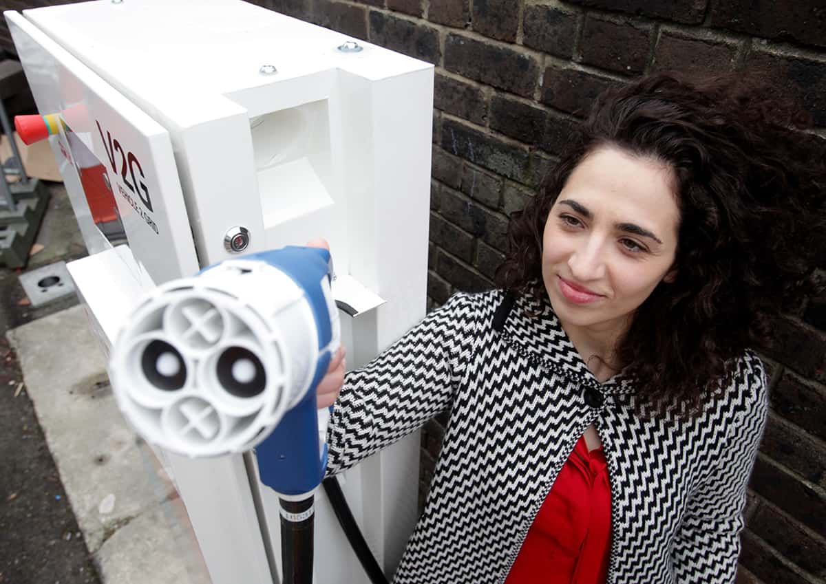
Two-way traffic Myriam Neaimeh believes that the energy stored in car batteries could provide power to local buildings or the electricity network to help balance demand. (Courtesy: Newcastle University)
Various strategies can flatten the fluctuations, such as tiered tariffs that incentivize drivers to charge up when electricity is cheap and plentiful. Smart chargers are already available to allow drivers to decide when to top up their battery, with more intelligent systems making it possible to automate charging to use cheaper electricity or more intermittent sources of renewable energy. “Just as consumers look at the price of petrol, people choose to charge their car when electricity is the cheapest,” says Frankland.
That view was backed up by a large-scale trial of smart-charging solutions that ran from 2016 to 2019 in part of the UK. The Electric Nation project, hosted by Western Power Distribution and led by EA Technology, recorded the charging behaviour of 700 drivers split into three groups. Two groups were able to charge whenever they wanted but had no information about the cost of electricity to guide them – resulting in them tending to charge their cars when they got home in the early evening. The third group, however, had access to costing information and smart chargers. “Even though there was a priority option for anyone who needed a full charge for the next day, most people in this group were happy to use smart chargers to manage when and how much they recharged their batteries,” comments Frankland. That modified charging behaviour led to a more gradual rise in energy demand, which at all times remained within the capacity of the local electricity network.
Some capacity problems may still emerge in areas where lots of people choose to buy an electric vehicle, but the data from these smart chargers would enable network companies to pinpoint the precise areas that need network reinforcement. “Any upgrades of the electricity network will ultimately be paid for by customers in their energy bills, so the best approach is to manage the demand and target the investment in the right places,” says Neaimeh.
Vehicle to grid
Further in the future, there is even potential for electric-vehicle batteries to provide a distributed energy-storage system that would help electricity providers to manage periods of high demand or surplus supply. This so-called vehicle-to-grid (V2G) technology exploits bi-directional chargers and automated control systems to store energy in car batteries when power is plentiful, and then release it back into the electricity network at times of peak demand.
Such flexible grid services could benefit businesses that operate fleets of electric vehicles, allowing them to cut their energy bills or even make extra income by providing grid services. For individual drivers, meanwhile, an electric car plugged into the mains supply could be used to store energy when electricity is cheap, and then provide power to the home when prices are higher. “V2G should help customers to reduce their energy bills,” comments Neaimeh. “We want the technology to support the grid while reducing the total cost of ownership of the car.”
One of the largest initiatives to test the viability of this V2G approach is the e4Future project, led by Nissan, in which up to 300 V2G chargers are being deployed with commercial fleet operators. “For the first time, this project is bringing together two big players – the energy companies and the automotive industry – who will need to work together if we are to decarbonize our power and transport sector,” says Neaimeh, one of the lead academics involved in the project.
According to the National Grid, the energy that could be provided by such V2G technologies will be part of a more general trend towards more localized energy sources, such as small wind turbines and solar-panel installations, which it believes will account for around 22% of the overall energy mix by 2050. Indeed, local authorities and commercial operators are already installing renewable-energy sources in car parks to generate energy for local buildings and provide power to electric vehicles. In Exeter, for example, solar canopies have been built on the top deck of two multistorey car parks in the city centre, a successful trial that has paved the way for a £1.3m project to install charge points powered by renewable energy across Devon’s towns and cities.
Fast charging
Major energy companies and specialist charge-point operators are rushing to install public charging stations on garage forecourts, motorway service stations and other public places. The UK already has 16 major charging networks and many more smaller or regional operators, which together provide more than 31,000 connection points. Most of these provide fast (generally accepted to be 7–22 kW) or rapid (25–99 kW) charging, with a few offering ultra-rapid services that can provide a full charge within about 20 minutes. “It is a very competitive market and lots of operators have installed as many charge points as they could in the best locations,” says Frankland.
But these rapid charge points are not necessarily the best solution for consumers. The electricity they provide is expensive, while reliability has been poor compared with other major infrastructure – at least in the UK. Each operator also runs different payment and membership schemes, which has made it difficult for drivers to access different networks and charging stations. “The public charging infrastructure should not be locked into a specific equipment or network provider, either commercially or technically,” a spokesperson for the Brussels-based trade association ChargeUp Europe told Physics World. “Open protocols should become the norm so that any operator and hardware meeting these minimum standards can compete on the market.”
More regulation is helping: operators must now offer the option of pay-as-you-go charging with a standard card payment, while roaming agreements are emerging in mainland Europe and the UK that exploit open protocols to enable seamless access and billing between providers. “Bringing together all the different apps and systems is quite challenging, but some of the larger charge-point operators are now starting to be a bit more consistent,” says Frankland.
Slow and smart charging
Given the current confusion around the plethora of public networks, it’s little wonder that most drivers prefer to charge their car at home. Slow charging at up to 7 kW benefits power-system management, and helps to maintain the long-term performance of the battery. “Superfast chargers are useful along travel corridors and in urban filling stations to allow drivers to quickly top up their batteries when they need to,” says Neaimeh. “But most charging demand should be met by installing low-power smart chargers where electric cars are parked routinely for long periods of time – at home and at work – to spread the demand for electricity and to make the most of renewable energy.”
Still, slow charging at home remains a challenge for drivers who do not have their own drive or garage – most notably the millions of city dwellers who stand to benefit most from switching to electric. According to Chris Pateman-Jones, chief executive of London-based charge-point operator Connected Kerb, around 34% of UK drivers park their car on the street while a further 28% have a parking space with no connection to a domestic power supply. “Our research indicates that most drivers want to top up in a regular, habitual way,” he says, “but that’s just not possible for the vast majority of people who don’t have easy access to a residential charging point.”
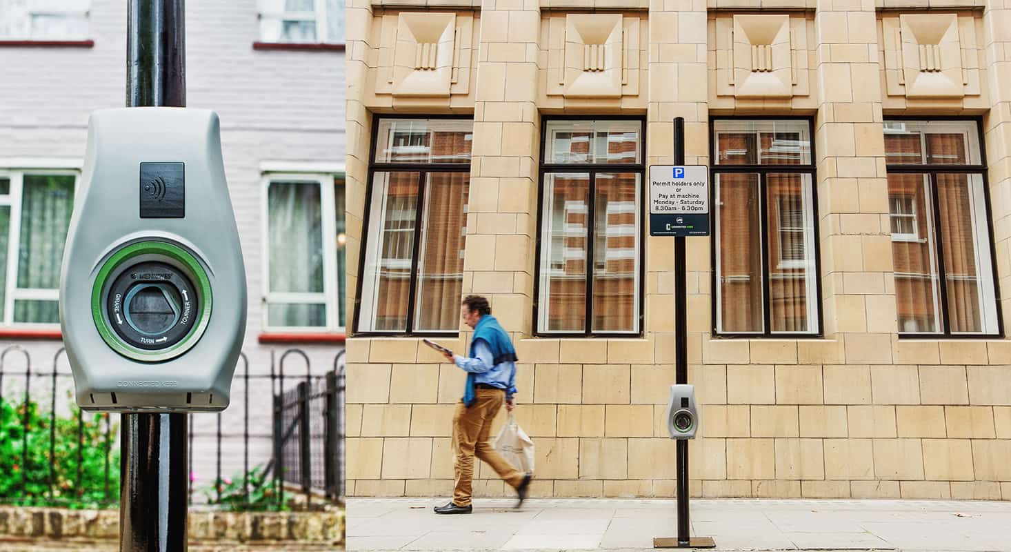
On-street solution Connected Kerb’s sockets can be fitted to existing street furniture, while the electric charger itself is installed below ground. (Courtesy: Connected Kerb)
Some operators have addressed this problem by installing charging points in street lamps, which are already connected to the electricity network. With a power rating of just 1–2 kW, however, it can take an hour to get enough power to drive 30 km, while trailing cables across the pavement is a clear trip hazard that many local authorities are keen to avoid.
Connected Kerb has therefore instead designed a series of dedicated on-street solutions that deliver slow charging at 7 kW. “Our approach is to separate the socket from the charger,” explains Pateman-Jones. “The socket sits above the ground, and is really small and discreet. The charger itself is installed below ground, which improves reliability because it is secure and protected.”
The beauty of this solution, says Pateman-Jones, is that it can be deployed at scale. “Rather than just installing two or three charging points in a neighbourhood, our technology can connect a whole street to the electricity network,” he says. “We exploit existing street furniture, such as parking posts and street bollards, which allows large numbers to be installed without ruining the visual look of the street. And wherever possible we put our kit in the ground when telecoms and utility companies are already digging up the roads.”
All the underground nodes are connected to the fibre network, making it possible to support smart-charging technologies as well as ancillary services, such as WiFi, environmental monitoring and potentially 5G. The modular design also ensures that the installed infrastructure is future-proof, with the underground chargers able to support the widely anticipated transition to wireless charging (see box below).
However, Pateman-Jones concedes that it will be a huge challenge to provide enough charging points in all residential areas. “Our estimates suggest that 62% of the driving population can’t charge their car at home,” he says. “Providing a charging point for one in four of those people would need 10,000 charging points to be installed every month for the next 15 years. The numbers are massive.”
For that reason Frankland believes that more diverse charging solutions will be needed in dense urban districts. “There could well be a move towards local charging hubs that would offer low-cost charging at 7–22 kW for a specific neighbourhood,” he says. “That approach could be easier to deploy in some localities, and would still allow residents to drip-charge their car for a few hours or overnight.”
But he is convinced that slow and smart charging will be the preferred option for many years to come. “You don’t need ultra-rapid chargers everywhere, and you don’t want them everywhere, because the cost of the electricity is higher and they put more strain on the local electricity network,” he says.
Instead, Frankland believes our charging behaviour will evolve to fit around our lifestyles. Fast forward to 2030, and we could well see lots of charging points in the workplace complemented by low-cost charging in supermarkets, hotels and other regularly visited leisure and retail sites. “You will be able to integrate your charging into your daily life,” Frankland predicts. “Rather than going to a petrol station every so often to fill up the tank, it will become second nature to charge while you park.”
A wireless future
On the move It costs SEK 6m (about £0.5m) to install 1 km of eRoadArlanda’s electric road system, compared with SEK 2m for a walking or cycle lane. (Courtesy: eRoadArlanda)
Trailing cables are one of the less attractive aspects of owning an electric car, but wireless charging technologies change all that. The most promising for urban drivers is induction charging, which transfers energy from a charging pad on the road to a receiver inside the car. “Induction charging is a fantastic technology that provides neater, cleaner charging for all users,” says Nick Dobie, one of the founders of London-based Connected Kerb. “It’s currently an expensive option, and not many vehicles are fitted with the right receivers, but it will change the face of charging over the next decade.”
Connected Kerb has already started to trial induction charging in specific use cases, in particular for drivers with disabilities that make it difficult for them to grapple with bulky cables. The company is also targeting taxi ranks – since taxi drivers would no longer need to take time out of their working day to top up at a rapid charging point – and shared vehicle schemes that typically have a dedicated parking bay.
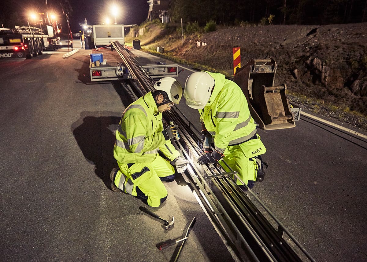
Meanwhile, some companies are investing in technology that can exploit wireless charging to top up a car battery while it is being driven. Qualcomm, for example, has teamed up with Renault to demonstrate this dynamic charging technology along a 100 m test track in France, showing that an electric van can charge at up to 20 kW while travelling at speeds of 110 km/h. The Swedish eRoadArlanda project has built 2 km of electric road that provides on-the-go charging at 200 kW – enough to power the battery of an 18-tonne truck.
The team behind eRoadArlanda believes that just 26,000 km of Sweden’s main roads would need to be electrified to provide an effective en route charging solution, which could be reduced by a factor of five if the power could be increased to 800 kW. “Electric roads can reduce the emissions and noise from existing road transport,” says project manager Sofia Lundberg. “The more traffic there is on the road, the greater the social and economic benefit.”
UK researchers have developed a new CT scanning method that produces the same image quality while also reducing radiation dose, according to a study published in Physical Review Applied.
The technique, called cycloidal CT, addresses two challenges, wrote a team that included senior author Alessandro Olivo of University College London.
“This new method fixes two problems,” he said in a statement released by the university. “It can be used to reduce the dose, but if deployed at the same dose it can increase the resolution of the image.”
About 5 million CT scans are conducted in the UK each year, while in the US, the annual number of CT scans is more than 80 million, Olivo and colleagues noted.
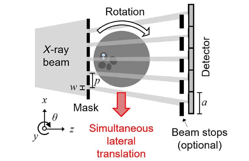
Schematic of cycloidal CT. (Courtesy: CC BY 4.0/Phys. Rev. Applied 10.1103/PhysRevApplied.14.014069)
To address the problem of radiation dose, the team developed the cycloidal CT technique, which splits a CT scanner’s full X-ray beam into smaller ones by putting a mask cut with small slits over the beam to create “beamlets” (the mask was made by electroplating gold strips onto a graphite base).
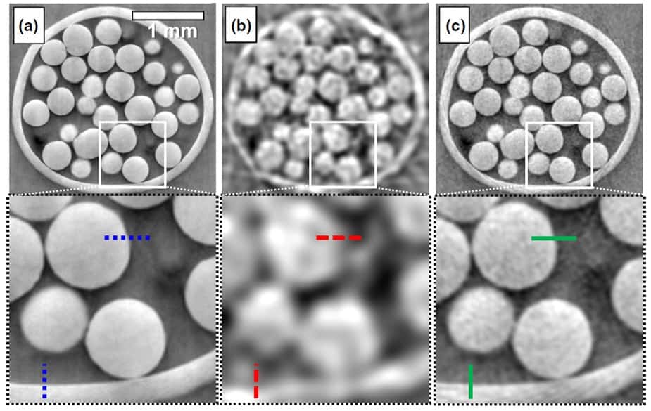
The investigators moved a scanning phantom made up of polyethylene spheres in a way that mimicked the X-ray beam rotation that occurs in a CT exam; the method included backward and forward motion. The current study compared this new technique with conventional CT scanning methods that involve directing a full X-ray beam onto the surface to be imaged.
Tomographic images of polyethylene spheres, acquired with (a) dithering, (b) rotation-only and (c) cycloidal sampling. (Courtesy: CC BY 4.0/Phys. Rev. Applied 10.1103/PhysRevApplied.14.014069)
“The use of beamlets enables a sharper image resolution, as the part of the scanner ‘reading’ the information from the X-ray is able to locate where the information is coming from more precisely,” the university statement said.
The cycloidal CT technique can be adjusted with changes to the mask, according to Olivo.
“The sharpness of the image can be easily adjusted using masks with different-sized apertures, allowing greater flexibility and freeing the resolution from the constraints of the scanner’s hardware,” he said.
The new CT scanning method shows promise for better patient care, lead author Charlotte Hagen, also of University College London, said in the statement.
“Being able to reduce the dose of a CT scan is a long-sought goal,” Hagen said. “Our technique opens new possibilities for medical research and we believe that it can be adjusted for use in medical scanners, helping to reduce a key source of radiation for people in many countries.”
A “quantum secret sharing” scheme that allows 10 parties to share information securely – the highest number so far – has been developed and demonstrated by researchers in South Africa. The protocol involves each party performing quantum operations on the photon without measuring its state and the team says it could help increase both the rate at which data is shared on secure quantum networks and how many parties can be involved in the sharing.
In the original quantum key distribution (QKD) protocol, two parties, known as Alice and Bob, communicate by exchanging photons polarized in one of two possible bases over an untrusted link, each varying the polarization basis of his or her transmitter or receiver randomly. At the end of the transmission, Alice and Bob reveal to each other which basis they used to measure the photons sent and received, but not the result of the measurements. Alice and Bob then announce their results for a sample of the photons in which they measured in the same polarization basis, to check that the emitted polarization always agrees with the received one. If it does, they can use the remaining photons that they measured in the same basis to form a secure cryptography key that allows them to communicate securely using conventional telecoms technology. A third party that intercepts the photons inevitably disturbs their state, so some of Alice and Bob’s measurements disagree and they know the line is bugged.
“OAM is like an infinite-sided dice”
While commercial QKD systems are available, the protocol has its shortcomings. One is that photon polarization has only two orthogonal states. These are traditionally used to represent 1 and 0, as in a conventional bitstream. Given the technical difficulty of sending and detecting isolated single photons, however, it is highly desirable to pack more information into each photon. In the new research, therefore, Andrew Forbes and colleagues at the University of Witwatersrand in Johannesburg encoded the data not in the polarization of the photon, but in its orbital angular momentum (OAM) –which can, in principle, be infinitely large. “Polarization has only two possibilities, just like a coin which can only be heads or tails,” explains Forbes, “OAM is like an infinite-sided dice.”
A second problem is that the traditional protocol allows only pairwise communication. “As soon as the receiver makes the measurement, the photon is destroyed,” explains Forbes. “There is fundamentally no way that you could extend that network from beyond just two people. Of course, the person who received it could repeat the whole exercise, but that’s not how normal networks work. You would like to be able to send your information to multiple people…and you’d like them only to be able to decrypt it if you trust them.”
To address this shortcoming, Forbes and colleagues have created a “pass-the-parcel” scheme by which photons in a superposition of 11 possible OAM states could be sent sequentially between 10 parties, eventually arriving back at the original sender. Each party performs one or more of a set of possible predefined operations on the OAM of the photon, but none of them measures its state. Only after the photon has completed its circuit does the party that originally emitted the photon (“the distributor”) measure its final state and compare it to the state of the photon originally transmitted.
Party-hopping photon
“In this final measurement, there’s a way to see whether people did something they weren’t meant to,” Forbes explains. Otherwise, each party now announces what operations it performed on the photon. “This photon, which has gone around all the parties, is now carrying all the information that each party imposed on it.”
If the parties trust one another, they can use this information to share a secret message without having to exchange any information of use to a third party. The actual states of the photon are only ever known to the distributor. Better still, says Forbes, it does not theoretically require that all the parties be trusted: “In our experiment we had 10 parties and we set it that all of them had to trust one another, but actually you can have anything less than 10,” says Forbes. “So, I could set it so that the information is spread across 10 people, but as long as two, three or four people trust one another, then those parties could collaborate to extract the key. That’s the power of the protocol: sharing and distributing a secret in a secure way, which QKD doesn’t allow you to do.”
“Andrew Forbes and his group have done outstanding work,” says Alan Willner of University of Southern California, “It’s adding on an important layer of what a real quantum system may use. This 11-dimensional, 10-party communication is really a great step forward.”
Physicists at the University of Colorado Boulder have become the first to observe a new phase of matter in liquid crystals. The “ferroelectric nematic” phase, which was first predicted to exist over 100 years ago, could find applications in many different areas, from new types of display screens to reimagined computer memory, says study leader Noel Clark.
“There are 40 000 research papers on nematics, and in almost any one of them you see interesting new possibilities if the nematic had been ferroelectric,” Clark explains. “Our discovery of one such liquid crystal could open up a wealth of technological innovations.”
Threads with order
Nematic liquid crystals display an odd mix of fluid- and solid-like behaviours, and get their name from the Greek word nema, meaning “thread” – a reference to the characteristic thread-like topological defects they contain. These defects are known as disclination lines, and they can be made of elongated molecules or colloidal particles. These molecules are polar, with one end carrying a positive charge and the other a negative one. In a traditional nematic crystal, half of these molecules will on average point in one direction (right, for example) and the other half in the other (say, left).
A ferroelectric nematic liquid crystal is more organized. Within specific patches or “domains”, all of its molecules point in the same direction. This phenomenon is known as polar ordering, and its appearance in nematic liquid crystals was first hypothesized in the 1910s by the Nobel laureates Peter Debye and Max Born. They predicted that if a liquid crystal were designed correctly, its molecules could spontaneously fall into a polar ordered state.
Shortly afterwards, researchers discovered solid crystals in which molecules did indeed point in uniform directions. The direction of these molecules could be reversed, from right to left or vice versa, when an electric field was applied – a property that inspired the name “ferroelectrics” because of similarities to ferromagnets. Despite much searching, however, a liquid crystal phase that behaves in the same way proved elusive – until now.
Strong polar order
Clark and colleagues observed their ferroelectric nematic liquid crystal phase in an organic molecule known as RM743. This molecule was created by another team a few years ago, in a study that showed that it exhibits a conventional nematic crystal phase at high temperatures. When cooled, however, another unusual phase appeared, and it is this phase that the Colorado researchers analysed using polarized light microscopy.
During their measurements, the researchers observed that when they applied a weak electric field to the material, a striking palette of colours developed towards the edges of the cell containing the liquid crystal. Overall, the team found that in this phase, RM734 is 100 to 1000 times more responsive to electric fields than traditional nematic liquid crystals. According to their calculations, this means that the molecules making up the crystals show strong polar order.
The researchers also discovered that distinct domains form spontaneously in the liquid crystal when it is cooled from higher temperatures. This suggests that there are patches within the materials in which the molecules seem to be aligned – a hallmark of a ferroelectric nematic fluid, Clark says. Surprisingly, the alignment was more uniform than expected for a fluid, in which entropy reigns and there should be a lot of disorder.
When the team analysed how well aligned the molecules were inside a single domain, they were “stunned” by the result. The molecules were nearly all pointing in the same direction, with only a few pointing in a completely different direction.
AI to screen potential new molecules
The researchers, who report their work in PNAS, say they are now busy trying to understand the mechanisms behind this alignment. “Our work suggests that there are other ferroelectric fluids hiding in plain sight,” says Clark. “It is important for us now to broaden the pool of molecules beyond the few (roughly five) now known to show this phase,” he tells Physics World.
The materials unearthed so far show the ferroelectric phase at elevated temperatures, so one goal of future research is to find room temperature materials, he adds. “We’re moving towards using artificial intelligence (AI) to screen potential new molecules without having to actually synthesise them. Indeed, 200 000 new molecular designs were made in the development and evolution of conventional nematic crystals LCDs, so we could avoid going through this.”
The thin-film materials being tested during development. (Courtesy: I Mathews)
Photovoltaic cells made from cadmium telluride (CdTe) – already widely used in solar energy generation – also excel at harvesting ambient light indoors, making them an excellent energy source for the fast-growing Internet of Things (IoT). This is the finding of researchers at the Massachusetts Institute of Technology (MIT) in the US and the Tyndall National Institute at the University of Cork, Ireland, who fabricated low-cost CdTe cells and measured their photovoltaic response when exposed to light from various sources, including LED bulbs.
At present, indoor IoT devices such as wireless sensors are typically powered by batteries. However, study lead author Ian Mathews says that photovoltaic cells would be better because of they require less maintenance and are cheaper and easier to make. In his view, these characteristics present a “significant market opportunity” for CdTe cells in particular, yet researchers have rarely tested their effectiveness at converting ambient light (from incandescent, compact fluorescence or LED bulbs, for example) into electrical energy. Instead, previous studies of indoor-light energy generation have mainly focused on rival photovoltaic technologies, such as silicon, III-V semiconductors, organic PV devices and perovskite materials.
CdTe has several advantages over its competitors in this respect. For one, its 1.4 eV electronic bandgap is a better match for typical indoor light spectra than silicon’s, meaning that it effectively absorbs low-level diffuse light from sources commonly employed to light homes and offices. Second, it is both cheaper and more stable than perovskite and organic PV materials. Finally, the processes required to manufacture it are relatively simple and rapid (10 times faster than traditional silicon-based technologies), and – thanks to years of commercialization for solar energy – well-established and optimized, too.
High light-harvesting efficiencies
In their work, Mathews and colleagues fabricated thin-film solar cells on low-cost commercially available soda lime glass with a transparent conducting oxide coating. They then sputter-deposited a n-type MgZnO buffer layer and p-type CdSeTe and CdTe layers on this substrate using a process known as sublimation. Next, they treated the entire film, which is about 5 microns thick, with CdCl2 to passivate the interface as well as any atomic defects. Finally, after treating the film with copper, the researchers deposited a metal back electrode onto it and delineated the ensemble into individual cells.
To test their cells, the team studied their photovoltaic response when exposed to standard solar energy testing conditions as well as a range of other light sources, including CFL and LED bulbs. Under the global standard spectrum of 1 W/m2 (AM 1.5G), they measured light harvesting efficiencies of 10%, while under low-level LED irradiance in the 0.2 to 2.9 W/m2 range (similar to 100 to 1000 lux levels in buildings), efficiency reached 17.1% – the highest value ever recorded for a CdTe device under ambient lighting.
Good in sub-optimal conditions and better than amorphous silicon cells
The results show that CdTe cells can operate in diffuse light conditions and therefore produce electricity in a wide variety of sub-optimal conditions, such as cloudy weather, reflected light and indoor settings. “In our experiments, we have found that they are very good at converting LED light into electricity and are better than the amorphous silicon cells currently employed in such applications,” Mathews tells Physics World. “They could thus be ideal for charging IoT devices.”
While the use of CdTe in household devices may trouble some consumers due to cadmium’s toxicity, the researchers note that the amount of the metal used in their photovoltaic cells is below the EU’s Restriction of Hazardous Substances (RoHS) limits. Full details of the work are reported in Journal of Physics D: Applied Physics.
The theme of the recent 2020 Joint AAPM|COMP Virtual Meeting was “Improving Health Quality. Increasing Global Impact”. The need to focus on global health is clear. While the burden of cardiac disease and cancer is rising disproportionately among low- and middle-income countries, such countries often have little or no access to quality imaging and radiotherapy technologies for timely diagnosis and effective treatment. There’s also a growing need for involvement of qualified medical physicists to ensure the safe delivery of high-quality care to patients.
“COVID-19 has taught us one lesson: global health is local health and local health is global health,” stated AAPM President M Saiful Huq. “Innovation in one part of the world, be it in the fight against COVID-19 or against cancer or any other disease, can benefit everyone across the globe. Collaborations between professionals from high-income and low- and middle-income countries can lead to innovations and development that can benefit all.”
In a dedicated symposium examining affordable medical physics technology for the developing world, speakers described a range of new and emerging low-cost healthcare systems.
Increasing imaging standards
Douglas Pfeiffer, a clinical medical physicist at Boulder Community Health, described a project to develop automated quality control (QC) for diagnostic and mammographic facilities.
“Implementation of regular QC programmes is poor for radiography throughout the world and for mammography, in many parts of the world,” he explained. “Regulations for quality assurance tend to be weak or non-existent.” And with diagnostic medical physics support minimal in many parts of the world, facilities often have little or no guidance on how to implement a quality assurance programme. “Imaging devices may go their entire lives without ever being tested,” Pfeiffer noted.
To remedy this situation, the IAEA set up a project to implement remote, automated and quantitative QC for radiography and mammography. The aim, explained Pfeiffer, is that one clinically qualified medical physicist will be able to support multiple facilities to ensure adequate and consistent imaging performance, which is important for areas of the world that are underserved by medical physicists.
In the proposed workflow, images of simple test objects are acquired locally and then either evaluated at the facility or transmitted to the medical physicist for remote analysis. The project team designed two inexpensive and easy to fabricate test objects – a radiographic phantom and a mammography phantom – both made from PMMA, copper and aluminium.
Images of simple test phantoms help provide automated quality control for radiography and mammography. (Courtesy: Douglas Pfeiffer)
The team also developed an automated tool for image analysis (ATIA). The ATIA software extracts relevant data from the DICOM header of the image, and then reports a series of measured and calculated values: signal-to-noise ratio; signal difference-to-noise ratio; modulator transfer function; normalized noise power spectrum; and detectability index. The results are exported in a CSV file for further analysis.
Pfeiffer explained that the detectability index is a new metric that helps directly relate phantom measurements to clinical performance. It can also be directly linked to a specific clinical task, such as detection of microcalcifications or small nodules, for example.
“The IAEA programme allows a clinically qualified medical physicist and the local technologist to remotely monitor clinical performance with minimal investment and time per unit. Due to its simplicity, training is straightforward.” Pfeiffer concluded. “Regular radiographic QC has been neglected, even in developed countries. This system makes it possible to perform QC on a regular basis, since it takes just a single exposure per unit and analysis can be automated.”
Low-cost TB screening
Relatively inexpensive imaging systems, such as X-ray and hand-held ultrasound scanners, combined with automated image analysis have enormous potential for countries with a lack of doctors. Bram van Ginneken from Radboud University Medical Center described two such systems – firstly a scheme to automate tuberculosis (TB) diagnosis. “Every day, about 4500 people die from tuberculosis,” he pointed out. “And the burden of disease is concentrated in Asia and Africa.”
In some aspects, van Ginneken said, TB has similarities to COVID-19. Both are diagnosed using RT-PCR (reverse transcription polymerase chain reaction) tests, which are expensive, time consuming and not always available. As such, for both infections, imaging also plays an important diagnostic role. One big difference, however, is that there’s an effective, $10 cure available for TB.
There is, therefore, a strong case for TB screening. And van Ginneken and colleagues are creating an automated screening process based on X-ray imaging. First, high-risk people receive a chest X-ray, which takes just one minute to record and process. If the X-ray looks suspicious, then the subject undergoes an Xpert diagnostic sputum test, waits two hours, and then receives a diagnosis. If TB is confirmed, they can be treated immediately.
Van Ginneken explained that the X-ray and Xpert machines can be easily set up, for example, on a bus that can travel between sites. He shared the example of a clinic in Zambia where the team placed their digital X-ray machine in a shipping container. He noted that even smaller systems are coming onto the market, such as a completely portable X-ray machine in a backpack. “It is quite heavy, but you can carry it anywhere,” he said. “There is an X-ray tube, a detector, a battery pack and a solar panel to charge the battery.”
To detect signs of TB on the X-ray images, the team developed computer-aided detection software called CAD4TB. The latest version of CAD4TB is based on deep learning, which can train classifiers to easily obtain very good performance. “It is already operational in over 45 countries throughout the world and we are screening about 5000 people per day,” said van Ginneken.
The team has also created a version of the software to detect COVID-19 on chest X-rays. “We have already received funding to test this CAD4COVID together with CAD4TB in a joint screening in Lesotho,” said van Ginneken. “The goal is to get people into the right part of healthcare system: find the severe COVID cases, less severe cases, TB cases and people who might have both diseases.”
Pregnancy risk prediction
Van Ginneken and colleagues are also applying deep learning techniques to help reduce maternal deaths by performing ultrasound imaging and analysis during pregnancy. “Every day, about 800 women dies as direct result of pregnancy,” he said. “99% of these deaths happen in low-resource countries.”
The scheme is based on a low-cost portable ultrasound device that can be directly attached to a smartphone for real-time image analysis. To analyse the ultrasound images and automatically detect any pregnancy risks, the team developed the BabyChecker software. This software uses deep learning to determine gestational age, predict delivery date, identify twins and detect a foetus in the breech position, which indicates a high-risk pregnancy.
While it is relatively simple to perform automatic measurements to determine gestation, it is essential to acquire the correct image frames. To achieve this without requiring extensive training, the team implemented a sweep protocol, in which the ultrasound probe is swept six times over the abdomen (three vertical, three horizontal). The resulting video contains all the required information.
“We have trained midwives in Ethiopia to perform these six sweeps, and saw that in two hours we can train somebody who has never used ultrasound before to perform sweeps in the right way,” said van Ginneken.
The deep learning software classifies every frame in the video, in real time, as one of six types: head, part-head, body, side view, detached transducer or other. These classifications can, for example, detect “head” frames located at the top of the sweeps, indicating a breech position, or find “head” frames at either end, suggesting the mother is having twins.
BabyChecker runs all of the deep learning networks in real time on the smartphone. The system also provides feedback during sweep acquisition to ensure the scans are performed correctly. “We found that countries with limited resources are very open to the use of AI to improve healthcare,” van Ginneken concluded. “With deep learning, we can rapidly develop these applications.”
Low‐cost arc therapy
Alongside medical imaging technologies, there’s also a real need to bring radiotherapy to lower-income countries. One approach, according to Magdalena Bazalova-Carter from the University of Victoria, could lie in the use of kilovoltage X-rays.
Magdalena Bazalova-Carter, Dylan Breitkreutz and colleagues are developing a low-cost kilovoltage arc therapy system. (Courtesy: Magdalena Bazalova-Carter)
While kilovoltage X-rays are common in diagnostic imaging, they are not the obvious choice for radiotherapy. It is difficult to deliver a high dose to deep-seated targets at kilovoltage energies, while low machine output compared with megavoltage linacs necessitates long treatment times.
“But there are advantage of kilovoltage X-rays,” Bazalova-Carter explained. “The shielding for a kilovoltage beam doesn’t have to be seven feet of concrete and the technology used is not as expensive. You could save a lot of money by using kilovoltage X-rays, which might be interesting for low- and middle-income countries.”
With this in mind, Bazalova-Carter and her former PhD student Dylan Breitkreutz, in collaboration with Michael Weil, have developed a kilovoltage arc therapy (KVAT) system. The KVAT source uses one-dimensional scanning of the electron beams onto the treatment anode, combined with collimation, to generate a linear array of focused kilovoltage beams that can be used to deliver arc therapy to generate conformal spherical dose distributions at depth.
For treatment planning, the team combined Monte Carlo simulations using the EGSnrc code with the Radify treatment planning system developed at McGill University. As the KVAT collimators are designed to deliver spherical dose distributions, while human targets are typically not spherical, the team used sphere packing to deliver dose to irregular targets.
Bazalova-Carter showed an example of a lung cancer treatment plan. Comparing dose distributions of the KVAT lung plan with a stereotactic ablative radiotherapy (SABR) plan showed that a higher volume received lower doses with KVAT, as expected, but met all Radiation Therapy Oncology Group (RTOG) dose constraints. Dose–volume histograms revealed that dose to the ribs was higher with KVAT; however, the oesophagus dose, for example was higher for SABR. She noted that KVAT treatment time is indeed still an issue, taking about 49 min to deliver a 12 Gy fraction.
The KVAT system with a 200 kV beam is currently under development by industrial partner Precision RT.
For women who undergo breast-cancer screening, the dread news of a suspicious finding on their mammogram or ultrasound scan is all too often compounded by an anxious wait for a follow-up exam that can take weeks to schedule. To streamline that disjointed patient journey and fast-track diagnosis, GE Healthcare is working with clinical partners and technology vendors to enhance the accuracy of 3D mammography – also known as digital breast tomosynthesis (DBT) – by exploiting a complementary imaging modality called contrast-enhanced spectral mammography (CESM).
A case study in this regard is the One-Stop Clinic at the Gustave Roussy Cancer Centre in France. In collaboration with GE, the Paris-based institute is rewriting the rulebook on breast-cancer screening. The goal: to give patients a definitive cancer diagnosis and treatment plan on the same day via multimodality investigations that dovetail the capabilities of GE Healthcare’s Senographe Pristina™ system for DBT imaging and CESM (the latter is known commercially as SenoBright™ HD). To date, more than 20,000 women have participated in the One-Stop Clinic, with 75% of those patients receiving a diagnosis on the same day.
Within this one-stop patient model – and indeed the wider clinical context – CESM has emerged as a key imaging technology for diagnosis and staging of primary breast cancer, offering superior sensitivity and specificity versus DBT alone. Deployed in tandem with DBT – in particular for women with denser breast tissue – CESM improves diagnostic accuracy through the injection of an iodinated contrast agent into the bloodstream (using the same protocol as for contrast-enhanced CT). In this way, the contrast agent enters general circulation but only enhances the region of clinical interest (a suspect lesion identified in the original mammogram) for subsequent imaging.
“The underlying principle of CESM is energy subtraction,” explains Remy Klausz, principal engineer for breastcare engineering at GE Healthcare Imaging. In brief, the CESM system acquires images at two different X-ray energies, with algorithms generating a recombined image – essentially subtracting the low-energy image from the high-energy image – to cancel out the images of background structures from regular breast tissue, enhancing areas of contrast uptake. “In this way,” Klausz adds, “CESM can demonstrate suspicious lesions otherwise ignored while significantly reducing false-positives – and without the considerable time and expense associated with follow-on functional imaging with breast MRI.”
Prioritizing the QA
From a commercial perspective, CESM continues to gain traction in the medical imaging community – though it’s also evident that not all mammography specialists are convinced. Some clinicians are uncomfortable with the injection of contrast agents in a mammography setting, while others are sceptical of CESM’s consistency – i.e. whether the modality will reliably demonstrate the presence or absence of iodine in suspect breast tissue time after time. Both, of course, are equally important: a suspicious area seen in the regular mammogram is likely to be non-cancerous if there is no contrast uptake, while enhanced contrast reveals a possibly cancerous lesion.
To address this cultural resistance, GE Healthcare has teamed up with CIRS, a US manufacturer of tissue-equivalent phantoms and simulators for medical imaging, radiation therapy and procedural training, to develop a simple yet comprehensive phantom for routine quality assurance (QA) of CESM systems. “Our motivation is to encourage more clinical users to adopt CESM,” explains Klausz. “Working with CIRS, we’ve come up with a versatile and easy-to-use phantom that, in just a few minutes, will give the radiologist full confidence that their CESM equipment is operating to specification.”
The original concept for the CESM phantom came from Klausz and his colleagues at GE Healthcare (see “Anatomy of a phantom”, below). After drafting the detailed technical specifications and concept drawings, Klausz approached the CIRS engineering management team with the idea for a joint development project. “CIRS is a leading provider of breast-equivalent phantom materials,” he adds, “so I had full confidence in their team’s ability to deliver what I was looking for.”
It took around six months from those initial discussions to first prototype, with CIRS granted full commercial rights to the phantom under the terms of the collaboration agreement. “Making a phantom is not our core competency at GE Healthcare,” explains Klausz. “Our motivation here is to provide a QA enabling technology to support wider clinical acceptance of CESM.”
Clinical and R&D customers can now purchase the resulting Model 022 CESM phantom on a commercial basis from CIRS. What’s more, the Model 022 uses the same frame geometry as the vendor’s DBT phantom, also some common parts, to further streamline QA protocols across DBT and CESM modalities.
Klausz concludes: “My recommendation would be to deploy the Model 022 phantom ahead of every CESM session. It’s just a simple visual check – no measurement is needed – to confirm that everything is working as expected from a machine point of view.”
Anatomy of a phantom
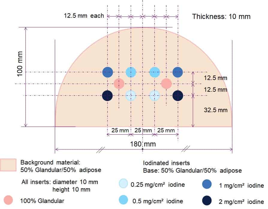
The Model 022 CESM phantom represents an average human breast in size and shape, demonstrating the presence or absence of iodine in tissues via different iodine concentrations and non-iodinated breast-tissue substitutes (see figure 1). The phantom consists of four slabs:
A 10 mm thick target slab is made up of breast-equivalent materials representative of a 50:50 ratio of gland and adipose tissue. The slab contains two sets of four plugs, each set comprising plugs with clinically relevant iodine concentrations of 0.25, 0.5, 1.0 and 2.0 mg/cm2 A fifth plug, made of 100% glandular tissue-equivalent material, is positioned in the centre of each plug group to mimic a glandular lesion.
The background slab, 25 mm thick, is made of two halves (100% adipose-equivalent material and 100% glandular-equivalent material) to test iodine separation from the background over a wide range of densities.
The top and bottom slabs are 10 mm thick, made from 100% adipose-equivalent material, and have rounded edges to mimic the realistic shape of a compressed breast.
Fig 1: The layout of the Model 022 CESM phantom has been arranged to match the shape and mounting of the CIRS DBT QA phantom. A magnetic fixture allows for repeatable alignment and positioning. (Courtesy: GE Healthcare and CIRS)