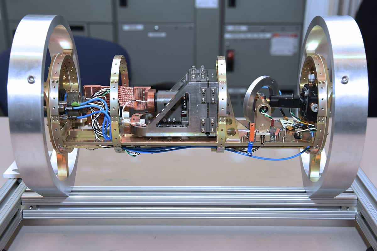
The future of photonics is taking shape along two converging coordinates as on-chip optical integration meets next-generation quantum technologies that exploit the exotic properties of quantum mechanics – entanglement, tunnelling, superposition and the like. The end-game: integrated quantum photonic devices, produced at scale, to controllably manipulate the quantum states of optical materials, opening the way to practical applications like quantum computing, quantum communications, quantum metrology and quantum imaging.
To make that quantum vision a reality – initially in an R&D context, though ultimately in terms of volume production and manufacturability – the German precision motion specialist PI (Physik Instrumente) has addressed a vexing, costly and long-term bottleneck in the testing, characterization and manufacturing of photonic devices down to the atomic scale.
Here Scott Jordan, head of the photonics market segment for PI, tells Physics World how the company’s Fast Multichannel Photonics Alignment (FMPA) technology – a set of firmware-level commands built into the vendor’s digital nanopositioning controllers, intelligent microrobots and stage controllers – can help developers to automate the optical alignment, test and assembly of quantum photonics devices while driving down production costs.
Why is automated active alignment – the foundation of FMPA – so important for the assembly of photonic devices?
There are growing requirements to align and position multiple optical components – for example, the lenses in smartphone cameras or the CCD chip itself – with nanoscale accuracy and economic efficiency. In integrated silicon photonics and next-generation quantum photonics, a multitude of tiny active and passive optical devices must be aligned for testing and packaging, starting at the wafer level. The common theme is multiple channels, multiple elements, multiple interacting inputs and outputs, multiple degrees of freedom – all need to be aligned and optimized multiple times throughout the manufacturing process.
If this is the problem, FMPA technology is part of the answer. Put simply, aligning the inputs and outputs of integrated photonic devices at industrial pace requires parallel optimization and nanoscale accuracy – not least in the coupling of on-chip waveguides with optical fibres. As we move into the quantum photonics realm, with its more complex production and test requirements, this parallelism will become increasingly critical to the process economics.
It sounds like the parallelism offered by FMPA has been a game-changer in photonics R&D and manufacturing?
FMPA is a huge advance over previous automated alignment technologies. Optical alignment is the single biggest cost/time sink in the testing and packaging of integrated photonic devices. In the short waveguides, typically millimetre-scale or less as increasingly deployed in silicon photonic devices, the input and output couplings can steer each other – so as one side is optimized, the other shifts slightly and needs reoptimization. In the past, this necessitated a time-consuming, serial sequence of back-and-forth adjustments of the input, then the output, repeating and iterating towards a global consensus alignment.
Similarly, when optimizing an angle, the transverse alignment would be impacted and would conventionally need to be reoptimized, again in a time-consuming serial loop. With FMPA, these interacting alignments can be optimized simultaneously to deliver a global consensus alignment, often in one go. In many cases, tracking and continuous optimization of all the alignments is also possible, allowing compensation of drift, curing stresses, and so on.
At a fundamental level, how do PI’s intelligent microrobots deliver optical alignment?
Scott Jordan: “Aligning the inputs and outputs of integrated photonic devices at industrial pace requires parallel optimization and nanoscale accuracy.” (Courtesy: PI)
At PI we make precision motion and nanopositioning technologies. Over the past four years, we have implemented a new generation of algorithms in the controllers for this equipment. These algorithms intelligently seek the optimum of a given optical figure of merit versus position. There are two types of alignment process: area scans to localize the main peak for a given parameter (e.g. optical power, modulation transfer function or modal purity) within a defined region, while parallel gradient searches efficiently optimize one or more such couplings at once – and optionally track them to mitigate drift processes and positional disturbances caused by temperature changes. In the case of a coupling between an on-chip waveguide and an optical fibre, for example, the manufacturer typically wants the alignment to minimize the light loss going from one element to another.
How have PI’s customers responded to FMPA technology?
The commercial launch of our parallel alignment technology was well timed. When we introduced FMPA four years ago, we found a niche with research and industry customers searching for faster optical alignment solutions to improve their production and test economics. A big driver is silicon photonic devices with arrayed-waveguide inputs and outputs – multiple optical channels that must be aligned simultaneously with optical fibres or other elements. To meet that need, we now have leading industrial players in silicon photonics – the likes of FormFactor Inc in the US, MPI in Taiwan and Tegema in the Netherlands – building high-throughput test and assembly equipment – photonic wafer probers and packaging-automation tools, respectively – based on our microrobots, positioning stages and advanced controls technology.
So FMPA is already being exploited to support early-stage device R&D in quantum photonics?
Absolutely. FMPA is at the heart of leading-edge photonic wafer probers that are being deployed by industry for testing of prototype quantum photonic devices – as well as optimizing the fabrication processes for such quantum devices. The probers are used to test the electronic and optical functionality of each photonic device on the wafer, so that the developer knows which devices are worth packaging. The same functional elements are routinely deployed on the benchtop level as well.
Is FMPA also being used by academic researchers working on quantum photonics?
We work with many pioneering academic customers to support development of next-generation quantum photonic devices. A case in point is a team led by Vlad Shalaev at Purdue University (West Lafayette, IN), who are using our FMPA systems to map, track and characterize novel single-photon quantum emitters that could prove fundamental to photonic implementations in quantum computing.
Essentially, the Purdue team has demonstrated high-brightness, single-photon quantum sources operating at room temperature – creating streams of fully randomized photons from atomic defects in nanoscale diamond films. To make use of the photons created by these defects, however, it is first necessary to collect them, guide them down an optical fibre, and measure them using a photon counter (typically tens of thousands of photons per millisecond).
With this in mind, we helped them build an open-source FMPA workstation comprising a very-high-precision xy positioning stage with an aperture in the middle – a set-up that is used to scan and lock onto the atomic-scale emitters so that they can be characterized. The workstation software took only eight hours to build from scratch, largely because all the functionality is incorporated into our motion controllers. All in, a neat example of PI’s alignment technologies being put to work in a fundamental research context that has demonstrated some world-leading results.
One of the enduring mysteries of physics is why the universe appears to contain much more matter than antimatter. An important clue has just been unearthed by the T2K experiment in Japan, which found a difference in what happens to muon neutrinos and antineutrinos as they travel through nearly 300 km of solid rock. In this episode the Durham University particle physicist Silvia Pascoli discusses the implications of the T2K result with Physics World’s Hamish Johnston.
Tomorrow (24 April) is the 30th anniversary of the NASA’s Hubble Space Telescope and the astronomy writer Keith Cooper has done a series of blogs for Physics World describing his favourite images. In the podcast he joins Margaret Harris for a lively chat about all things Hubble. Their wide-ranging discussion begins with how the telescope was saved from ruin in its early days and ends by pondering the mission’s future.
Andrés Castellanos-Gómez is a materials researcher who combines tradition with the cutting edge. His group at the Materials Science Institute of Madrid is interested in complex oxides, which are grown epitaxially on the surface of crystals before being isolated from their substrate by etching. Alongside this long established method, the team deploys techniques from the emerging field of 2D materials to create 2D heterostructures held together by Van der Waals forces.
Straintronics innovator: Andrés Castellanos-Gómez. (Courtesy: James Dacey)
Employing this combined approach, Castellanos-Gómez’s group creates prototype “straintronics” devices – tuneable electronic components whose properties change upon the application of strain. One example is the concept of a camera that could be switched from detecting visible light to infrared light simply by applying strain to the pixels within its sensor.
Castellanos-Gómez describes this research in this interview with Physics World, recorded recently before Spain’s lockdown began in March. He also explains how his team works with a network of other European research groups under the EU’s Graphene Flagship programme.
Find out more about the materials research taking place at the ICMM in this video profile we shared last week. Also take a look at the Physics World Nanotechnology Briefing, published in April 2020. This free-to-read collection celebrates how nanotechnology is playing an increasingly important role in applications as diverse as medicine, fire safety and quantum information.
An enigmatic object once thought to be a massive exoplanet is more likely to be the remnants of a catastrophic collision between two comet-like bodies, two US astronomers have shown. Andras Gaspar and George Rieke at the University of Arizona made the discovery after re-analysing observations of the Fomalhaut system made by the Hubble Space Telescope (HST). Their proposal could improve our understanding of how orbiting bodies can destroy each other, even in more peaceful star systems.
In 2008 a team of US astronomers announced the discovery of a massive exoplanet orbiting the bright star Fomalhaut. Unusually, the new exoplanet was imaged directly, using observations from the HST, rather than having its existence inferred from its effects on the orbit or brightness of its parent star. Since then, however, the object has thrown up a few puzzles for observers. Unlike planets with similar masses, it is optically bright but emits virtually no infrared radiation. In addition, it appears to have far less gravitational influence on Fomalhaut’s debris disc than astronomers first predicted, suggesting that Fomalhaut b is much less massive than initially thought.
Gaspar and Rieke have now shed new light on the mystery by revisiting previous data from the HST. Through this analysis, they concluded that Fomalhaut b has both expanded and faded since its discovery, and also appears to be on a trajectory that would see it escape from its host star. This would only be possible if Fomalhaut b were not a planet after all, but a dispersing cloud of fine dust being pushed away by energy radiated from its host star. The duo further strengthened their hypothesis by creating simulations of expanding dust clouds under similar radiation pressure, and demonstrating that the clouds’ behaviour was consistent with the HST’s observations.
Gaspar and Rieke believe that the only plausible explanation for their proposed cloud’s origin is a recent catastrophic collision between two comet-like planetesimals, each around 200 km across. Such a collision would be a rare event, occurring perhaps once in every 200,000 years in a system like Fomalhaut, which has long since passed through its violent early formation stages. This suggests that Fomalhaut’s planetesimals could be undergoing a reshuffling, driven by the evolving orbits of other, as-yet undetected planets in the system.
The duo now hopes to learn more about the circumstances of Fomalhaut b’s formation by directly imaging the inner regions of its host system, which will be possible after the long-awaited launch of the James Webb Space Telescope. By identifying the orbits of actual exoplanets in the system, and exploring the architecture of Fomalhaut’s debris disc in more detail, their future research could produce new insights on how such major events could occur in seemingly uneventful star systems.
A few years ago I wrote an account about a physicist, who was then alive but has since died. I won’t reveal who he was. Then last year, a woman sent me a letter saying that the physicist had been abusive to her and to other women, and that they resented my “hagiography” of the man. The women were troubled by my “mansplaining” and by my deference to the man’s reputation. It would have taken me only “a meeting and a phone call”, she continued, for me to realize that I should have nuanced my “worshipful” picture.
Naturally, I was upset. I had indeed spoken with people who had told me privately that the physicist had been a “womanizer”. One of them put it jocularly, saying that the man had had some issues with “the ladies”.
The woman’s letter forced me to face my responsibility for not having followed up on those remarks, as well as my responsibility for what to do now.
Cosby parallel?
As a historian and biographer, I am not alone in facing this difficulty. So are numerous writers and scholars, for instance, who wrote about the beloved American TV entertainer and cultural icon Bill Cosby. In the 2000s several women accused him of drugging and assaulting them. By the 2010s more than 60 women had made accusations, all of which he denied. In 2018 Cosby was tried and convicted of three counts of assault and sentenced to between three and 10 years in prison.
While all this was going on, numerous glowing articles had appeared about Cosby, including one by the bestselling author Ta-Nehisi Coates. In 2008 Coates wrote his first major article for a national magazine – The Atlantic – which happened to be about Cosby’s moral and political influence. In 2014, as accusations against Cosby mounted, Coates wrote another article for The Atlantic asking himself why he had made only a “brief and limp” mention of the accusations in the previous article, despite having known about them and believing the women. In the latter piece, Coates did not seek to absolve himself; instead, he tried to understand why he had been “reckless”, as he put it, for not having paid attention.
One reason, he wrote in 2014, was that the 2008 Atlantic article had been his break-out chance, and Coates was loathe to possibly anger his editors by including material that seemed extraneous to what they had commissioned him to do. He also feared that readers wouldn’t believe that a man who seemed to embody American values and virtues could be guilty. The allegations were hearsay back then, he reasoned, and pursuing them would require a lengthy investigation that he wasn’t prepared to take on. Still, Coates concluded, his not looking more deeply into the allegations was an admonition “to always go there, to never flinch, to never look away”.
So was my case similar? In some ways, no. I had had only vague hints of abusive behaviour, and none of it involved drugs and rape. Also, my subject was a physicist and the context was science.
But those of us who write about science have other temptations. Captivated by brilliant work and professional accomplishment, we concentrate on the accomplishments – not on the personal lives of scientists, which are as messy and complicated as anyone else’s. It’s easy to be blinded by the impression that physicists behave differently from, say, celebrities, media moguls, famous journalists, athletes or politicians. We call it a moral duty not to disparage the reputations of anyone without proof, and know that pursuing such proof can require training that we lack. All that can cause us to overlook the misconduct of individuals whose predatory behaviour becomes public – as has happened in the physics community over the last few years.
Hearing voices
I exchanged a few letters with the woman and went to meet her. I did not defend myself, but relayed my temptations to look away. She seemed to understand. But what was my responsibility now?
After months of brooding I mentioned the dilemma to a science historian. Her response was that it is not up to me to speak for this woman, and that I should try to persuade her to speak for herself. That woman, and others in her position, need the opportunity to have their voices heard and situations known. I followed the suggestion, but the woman declined. She was not a writer, she explained, and it would be a highly personal story that it would be hard to make meaningful to others; besides, who would publish it?
There seems no good place to bring injustice to light, no fair way to put it, no adequate language in which to discuss it
I understood, but was still troubled. I would be irresponsible if I wrote a one-sided account of an episode about which I had only hearsay. With the person in question now deceased, I would certainly end up misrepresenting the situation. I would also be guilty if I ducked or simplified the issue. The woman’s situation seemed impossible for me to reckon with because it was difficult even to frame. There seems no good place to bring what injustice there is to light, no fair way to put it, and no adequate language in which to discuss it.
The critical point
The woman’s letter reminded me of the responsibility that those who write about science – or about any community – have for revealing whole, not partial truths. It also reminded me of the temptations to become complicit. What has attracted us to study the community in the first place, we need to ask, and to what temptations and pitfalls might this attraction lead us to succumb? Writing this column, without identifying the person, is the best way I can think of to be responsible in this case.
The word “iconic” doesn’t do the Pillars of Creation justice. Originally imaged in 1995 by Hubble’s Wide Field and Planetary Camera 2, the colourful Pillars signalled a fundamental shift in the public’s perception of the space telescope’s worth and abilities, which had been tainted by the controversy of its initially blurred vision. This 2014 reshoot, taken using the Wide Field Camera 3, show the Pillars in all their glory: three towering columns of molecular gas, each several light years long and found at the heart of the Eagle Nebula, which is located around 5700 light-years away within the Milky Way.
Amazingly, the columns are the result of erosion. Just as wind sculpts rock columns in the desert, the torrents of ultraviolet radiation emitted by hot young stars that have formed within the nebula shape the clouds of gas around it. The Pillars of Creation are a majestic ode to our origins in a similar molecular gas cloud, 4.6 billion years ago.
A magnetometer with unprecedented imaging sensitivity promises to bring electromagnetic induction tomography to the clinic. The device, developed by researchers at University College London, images a sample’s conductivity by measuring the magnetic signature of eddy currents induced within it. By demonstrating the technique in a magnetically unshielded environment, the team showed its potential for biomedical applications – for example, to diagnose and guide treatments for atrial fibrillation (Appl. Phys. Lett. 10.1063/5.0002146).
Atrial fibrillation is a life-threatening cardiac arrhythmia in which the electrical pulse that governs the heart’s rhythm is disrupted. The precise causes of the condition are still mysterious, but a leading theory proposes that the disruption is due to anomalies in the electrical conductivity of the heart’s tissue.
“Specifically, clusters of cells in the cardiac muscle become more conductive than they should be,” says Luca Marmugi, who co-authored the research with Cameron Deans and Ferruccio Renzoni. “This creates a sort of ‘short circuit’ in the heart, that prevents the correct propagation of the electrical pulse controlling the heartbeat.”
Left to right: Cameron Deans, Luca Marmugi and Ferruccio Renzoni. (Courtesy: UCL Laser Cooling Group/Henry Bennie, UCL/Ferruccio Renzoni)
Monitoring the heart’s naturally generated electrical currents via the magnetic fields that they produce is routine, constituting the well-established field of magnetocardiography. But locating the abnormally conductive cells thought responsible for atrial fibrillation requires a technique that can image the heart’s passive electrical properties as well. Electromagnetic induction imaging (EII) is such a technique.
In EII, a radiofrequency (RF) alternating electric field is used to induce eddy currents in the target under investigation. Measuring the strength of the magnetic field associated with these eddy currents reveals the target’s electrical properties.
But although EII is a proven technique in geophysics and non-destructive testing, biomedical applications have been stymied by the inadequate sensitivity of available magnetometers. To image heart tissue, for example, EII sensors need to detect conductivities of less than 1 siemens per metre (S/m). Even under ideal conditions, atomic magnetometers – the most sensitive instruments developed so far – bottom out at four times that value, and in unshielded, magnetically noisy environments the detection limit rises to 50 S/m.
The device that Marmugi and colleagues used to close this sensitivity gap is based on the same basic instrument employed in those earlier attempts, but with some important refinements. Central to the technique is a vapour cell containing rubidium-87, which the researchers excite into a spin-polarized state with a laser. Meanwhile, the RF field that induces eddy currents in the target simultaneously drives Larmor precession of the Rb atoms’ magnetic moments, making their spin axes wobble like unbalanced spinning tops. The presence of an additional external magnetic field alters the rate and phase of precession, and can be read off in the polarization angle of a linearly polarized laser beam shone into the cell.
In principle, the sensitivity of the baseline version of the device could be improved by boosting the power of the RF field, thereby increasing the induced current and strengthening the resulting magnetic field. In practice, however, raising the RF field strength also broadens the Rb atoms’ spectral lines by a phenomenon called power-broadening – with the overall effect of diminishing the instrument’s sensitivity.
The researchers sidestep this problem using two identical RF coils, which they operate in anti-phase. By placing the vapour cell midway between the two coils, where the fields cancel out, they can avoid power broadening even while ramping up each coil’s individual output. Locating the sample to be imaged nearer to one coil than the other, induces in it strong eddy currents from the increased driving field.
Combined with some other hardware modifications and data-retrieval methods that Marmugi and colleagues have developed over the last few years to handle stray fields, the improved sensitivity of the dual-coil setup enabled them to image a sample with a conductivity of 0.9 S/m. The small size of the sample (5 ml), and the fact that their experiment was unshielded (in a laboratory bathed in the fluctuating magnetic fields from three of London’s main underground train lines) bodes well for the technique’s application to atrial fibrillation.
Next, the researchers intend to perform pre-clinical and clinical studies before rolling out their device to patients.
“In principle, the instrument could be deployed very broadly, from clinical wards to surgical theatres,” says Marmugi. “Thanks to its intrinsic safety, non-invasiveness, and its small power requirements, one could also envisage a more capillary diffusion, potentially – in the longer term – down to GP practices.”
Diamonds are well known as the gem for marking engagements and other special occasions, but the huge influence of this material in industry is all around us too. Diamond is used, for example, as a tool for machining the latest smartphones, as a window in high-power lasers used to produce automotive components, and even as a speaker-dome material in high-end audio systems. However, there is a new application on the horizon that could be even more profound – that of diamond quantum technologies.
At the turn of the 20th century, theoretical and experimental scientists were grappling to understand how the universe worked at very small scales. The results of this turned into the field of quantum mechanics, which has led to innovations – such as lasers and transistors – that impact our daily lives. These so-called “quantum 1.0” technologies rely on the effects of quantum mechanics, but now in the 21st century, scientists around the world are trying to develop the next wave of innovations. “Quantum 2.0” technology will rely on manipulating and reading out quantum states, and will typically exploit the quantum effects of superposition and entanglement.
The challenge of developing quantum technology is that quantum states are so fragile. Ideally these states would be isolated from everything else, but to make them useful you need to interact with them. Some applications can take advantage of this fragility – for example, in developing highly sensitive sensors – but they still need a degree of isolation to be controlled in the first instance. This balance between control and interaction is the fine line quantum scientists are having to traverse.
Quantum technology research covers quantum computing, simulation, communication and sensing, with potential impacts in healthcare, the automotive industry and the development of new materials, to name a few. Currently a wide range of different technological solutions are being investigated for these new applications, such as trapped ions, superconductors, quantum dots, photons and defects in semiconductors. Each technical solution has different pros and cons. Trapped ions have exquisite quantum properties but are challenging to integrate, whereas circuits of superconductors can be fabricated but can only operate at cryogenic temperatures. This is where materials like diamond come into play as they offer a compromise by being solid-state – making it easier to integrate into devices – and operational at room temperature.
Quantum diamond
A lot of research into diamond has focused on identifying the hundreds of different defects that can be found within the carbon lattice. One such imperfection is the negatively charged nitrogen-vacancy (denoted as NV) defect (see box below). In 1997 Jörg Wrachtrup and colleagues at the University of Technology Chemnitz in Germany showed that a single NV defect could be manipulated and provide an optical output at room temperature (Science276 2012). This discovery sparked the field of diamond quantum technology (see Nature505 472 for a more detailed history). The process is called optically detected magnetic resonance (ODMR) and, with the NV defect, it is observed when measuring a change in fluorescence after shining green light on a single NV defect, or on an ensemble of them, while scanning an applied microwave field. When the field hits resonance with the spin quantum numbers (ms) causing a transition from ms = 0 to ms = ±1, a decrease in fluorescence is observed. So by measuring the intensity of the fluorescence, you can read out the spin state of the defect.
The NV defect
Imagine a perfect diamond lattice of repeating carbon atoms. Remove two adjacent atoms, then replace one with nitrogen (bright blue in figure), while the other remains a “void” or vacancy (pale blue). This is the neutral nitrogen-vacancy defect in diamond, and it can have four different crystallographic orientations. Should there be another defect nearby in the lattice that has an electron with higher energy – usually a substitutional nitrogen that has no vacancy – this electron will transfer to the nitrogen-vacancy to give it a negative charge.
The electrons associated with the negatively charged nitrogen-vacancy (NV) defect occupy the dangling bonds around the vacancy such that their energy levels behave similarly to those in a trapped ion.
These NV defects have a special combination of energy levels, such that whatever ground-state spin an electron starts in, once the crystal is illuminated with green light, it will cycle through energy levels and is statistically more likely to enter the spin state ms = 0. Cycle the electrons around this loop enough times and the spins will effectively be aligned. Once in this ms = 0 ground state the NV defect can be manipulated to do a quantum experiment by applying microwaves and further pulses of light. The readout process relies on the same phenomena, exploiting the fact that the amount of light emitted by the defect is “bright” or “dark” depending on its ground-state spin when measured.
Over the next decade, a few academic groups around the world picked this work up, hoping to use diamond as a quantum bit, or “qubit”, in quantum information devices, such as quantum computers. This work was undertaken using a single, unique natural diamond dubbed the “Magic Russian Diamond”. Meanwhile, many companies began developing new techniques to produce high-purity synthetic single-crystal diamond for industrial applications using microwave-assisted chemical vapour deposition. In the early 2000s, for example, staff at our firm Element Six showed that it was possible to grow diamond with fewer than five impurity atoms per billion carbon atoms. In such diamond, nitrogen is the predominant impurity, and isolated NV centres can be probed. Eventually, in 2006 when this material’s quantum properties were tested, they were shown to be comparable to the Magic Russian Diamond. The finding was significant because the new synthetic diamond could be mass produced (see figure 1) and therefore allowed many more academic groups to have access to the material and start to understand how to control and use the NV defect.
1 Depositing diamond
(Courtesy: Element Six)
High-purity single-crystal synthetic diamond plates produced by microwave-assisted chemical-vapour deposition. Each diamond is approximately 4 × 4 × 0.5 mm.
At this point, much of the academic research was focused on fundamental quantum physics and quantum computing. However, in 2008 work taking place in the group of Wrachtrup – who was now at the University of Stuttgart, Germany – and in Mikhail Lukin and Ron Walsworth’s groups at Harvard University in the US, proposed and showed that diamond could be used to make a magnetic sensor, in which the brightness of the NV defects’ optical output depends on the strength of the magnetic field. Since then, many new applications using the NV defect have been proposed.
The reasons why diamond provides such a wonderful host to quantum defects come from its crystal structure. For example, diamond is a wide band-gap material, meaning that it can host a range of defects with transition energies in the optical regime, enabling the defects to be manipulated with readily available lasers. As carbon has a low atomic mass and very stiff interatomic bonds, it has a high Debye temperature (the temperature of a crystal’s highest normal mode of vibration), which makes the interaction of the NV centre with the vibrational modes of the surrounding lattice unusually weak, even at room temperature. Diamond also has a naturally low concentration of nuclear spins (carbon-12 has a nuclear spin of 0 and there is only 1.1% carbon-13 (spin –1/2) in diamond). This reduces the likelihood of the quantum states “decohering”, when the spin is no longer in the desired state. Quantum states can also decohere via spin-orbit coupling – a relativistic effect where the spin of a charge interacts with its orbital motion. But because the NV defect has weak spin-orbit coupling, there is limited decoherence and the spin state lasts for longer. Together, these properties mean that it is possible to fabricate a diamond with a spin decoherence time of milliseconds at room temperature. And as well as diamond being a good host for spin defects, the NV centre is also particularly special in that its electronic energy-level structure means that the electronic spin associated with it can be manipulated simply by shining green light on it.
Despite these desirable features, the NV defect in diamond is not perfect. In an ideal world, all the photons emitted would be at 637 nm for them to be quantum mechanically indistinguishable. However, most of the photons emitted are at different wavelengths, from 637 nm to 800 nm, due to phonon interactions, which provides a challenge for some applications. Other difficulties are that diamond is not as easily processed as materials such as silicon – it is much harder to etch structures in diamond to improve optical collection from the defects, and high-purity single-crystal diamond has only been made up to around 10 mm2. These limitations of diamond and the NV defect have led to scientists looking for alternative defects in diamond and in other wide band-gap materials such as silicon carbide (SiC) and zinc oxide (ZnO). However, while a few other defects in diamond and other materials have been identified to have useful properties, no-one has found one that rivals diamond’s NV centres.
Diamond devices
One of the benefits of a diamond-based quantum device is its simplicity. A basic device can be fabricated from a green light source, a diamond, a small microwave source and a photodetector. This is because effective optical initialization and the readout process of NV spins do not require specialized narrow-linewidth lasers – even a simple green LED can be used. Furthermore, because of the wavelength of light being detected (637–800 nm), low-cost, off-the-shelf silicon photodetectors can be used. An offset magnet is also used to provide a field of a few millitesla, which separates the energy levels of the four different possible crystallographic orientations of the NV defect, allowing them to be probed independently. Lastly, the microwave frequencies that are used are roughly 2880 MHz. All of these components can be bought off the shelf for a few thousand pounds, and instructions to build such a room-temperature quantum device are readily available and suitable for a first-year physics degree demonstration (American Journal of Physics86 225). However, while this set-up shows the principles of operation, it clearly does not show the enhancements in performance you would expect from a quantum device.
Extensive engineering is required to maximize performance in a particular application. For example, if you require ensembles of NV defects, there is a trade-off in performance between the concentration of NV defects in the diamond and the spin coherence time. If the NV defects are too close together, interactions with nitrogen – which donate the electron to form the negative NV charge state – reduce the spin-coherence time. However, if they are too far apart then it is harder to provide each defect with the same uniform illumination, magnetic field and microwave field, as well as collect as much of the luminescence from the NV defects at the detector.
The original motivations for academic work on diamond-based quantum systems were to investigate fundamental physics and to consider using diamond in a quantum computer. This is the most demanding of all the diamond quantum applications as it requires the most stringent performance of the defects. Specifically, each defect needs to behave in exactly the same way, emitting light at precisely the same wavelength. Unfortunately, imperfections – such as dislocations in diamond’s crystal structure – create strain, which shifts the emission wavelength of the light enough to make two NV defects distinguishable. This can be countered by applying an electric field near a defect that can be “Stark tuned” such that the emission wavelength is the same – however, changes in the local charge configuration surrounding the NV can still change during a measurement causing a wavelength shift. Despite these potential hurdles, several breakthrough results have been achieved with diamond, including the first successful “loophole-free Bell’s inequality test” in 2015 (Nature526 682), and the longest spin lifetime without the use of any cryogens. Building on these achievements, a 10-qubit register that can store quantum information for up to 75 s has recently been demonstrated (Phys Rev. X9 031045).
As part of a current project, Ronald Hanson’s group at the Delft University of Technology in the Netherlands is using the NV defect in diamond as a “quantum repeater node” in a 100% secure quantum internet. In such a network, the nodes are quantum mechanically entangled to build up a chain from the source to the receiver so that quantum information can be transmitted over large distances. Such a demonstration is a challenging target, but there are also many nearer-term applications using the fragility of the quantum states.
Another emerging application is the diamond-based maser. Invented in the 1950s, masers are not as widespread as lasers but nevertheless have many invaluable applications. Masers are used in radio astronomy and deep-space communication due to their high gain and very low noise. Being so stable over short timescales, they are also used as oscillators, which enables high-precision timing required for global positioning systems.
However, current maser systems can be bulky and complex, and can also require cryogenics, which limits where they can be deployed. A breakthrough in 2018 (Nature555 493) demonstrated the world’s first continuous-wave (CW) room-temperature solid-state maser using the NV defect in diamond. This maser works using the same energy levels used in magnetometry but a magnetic field of greater than 0.1 T is applied, which pushes the ms = –1 energy level below the ms = 0 energy level via the Zeeman effect. Choosing a particular magnetic field strength, you adjust the energy gap between the levels and thereby select the operating frequency of the maser. Then, pumping the diamond with a green laser puts the electrons in the ms = 0 energy level and thereby creates a population inversion.
To get maser operation requires the diamond to be in a high Q cavity, the applied magnetic field to be stable and homogenous, and the temperature fluctuations of the diamond to be minimized. If these engineering challenges can be solved, compact diamond masers may pave the way not just for existing maser applications, but also for new opportunities that have yet to be considered due to the limitations of current maser technology.
Detecting with diamonds
As mentioned, in 2008 the concept of using the NV defect in diamond as a magnetic sensor was first proposed, with practical demonstrations appearing in 2009. In a diamond magnetic sensor, the luminescence collected does not have to be at a particular wavelength and therefore all emission in the phonon sidebands from 637 nm to 800 nm can be collected as signal. A diamond magnetic field sensor in principle has many advantages over other sensor technologies. For example, it is an intrinsic vector sensor by virtue of the fact that it is sensitive along the axis of the NV defect, which means that the four different NV orientations can be used to reconstruct a vector field. It also has a massive bandwidth, being sensitive to magnetic fields over several orders of magnitude, and – unlike other technologies such as vapour cells – it does not require special magnetic shielding.
A diamond magnetic field sensor in principle has many advantages over other sensor technologies
There are also different modalities of NV magnetic sensor depending on how many defects are used in sensing. Due to the NV defects’ properties, strong electronic dipole luminescence from single ones can be easily measured, allowing magnetic fields to be measured on the nanometre scale. Competing technologies such as magnetic resonance force microscopy can also do this, but as they are intrinsically magnetic, they perturb the system they are trying to measure. Many groups are therefore using NV-based tools for material characterization, such as investigating magnetic materials that contain skyrmions. Start-ups such as Qnami, based in Switzerland, are trying to capitalize on these developments by selling ready-made diamond probes containing NV defects.
Using ensembles of NV defects can make the device more sensitive but lower its spatial resolution. As a compromise, a few microns of high-NV-defect-containing diamond on top of a high-purity diamond can be used to image magnetic fields where the thickness of the NV-containing layer determines the spatial resolution. This technique has been used to measure the magnetic signature from a meteorite, which could then be used to establish the magnetic field when the solar system was formed. Adding even more NV defects into the diamond to make a bulk diamond sample containing NV defects throughout can push sensitivities into the picotesla regime.
2 Jam-resistant GPS
(Courtesy: Lockheed Martin)
Lockheed Martin’s diamond magnetometer for a GPS that does not rely on an external source that can be jammed. The system is currently the size of a shoebox but can be shrunk down to the size of hockey puck.
Using such a bulk magnetometer, a team at Lockheed Martin – the US-based aerospace company – has been developing a diamond magnetometer that can be used as an alternative GPS that does not rely on external signals (see figure 2). The technology works by using the vector capability of a diamond magnetometer to sense the strength and direction of Earth’s magnetic field. Given that Earth’s field varies depending on where you are on the surface, this fact can be used to position yourself without relying on an external source that can be jammed. Even early prototype systems have demonstrated this and, while not as accurate as satellite-based GPS, they will likely work alongside existing technology to provide redundancy.
The sensor can also be used in reverse to detect radio-frequency (RF) fields. In this configuration, a magnetic field gradient is placed across the NV-containing diamond in a controlled way, which then provides a known Zeeman shift of the energy levels. When a microwave signal of unknown frequency is applied, a magnetic resonance appears at the position that corresponds to that frequency. The big advantage of this approach is that you can measure across a whole frequency spectrum – more than tens of gigahertz – in one measurement and with high resolution. This technology could be used in 5G networks to prevent interference between neighbouring cell towers.
Diamond-based quantum technology also has applications in the medical industry. A few groups around the world, as well as the start-up NVision based in Germany, are using diamond to enhance magnetic resonance imaging (MRI) – turning it from an anatomical to a molecular imaging modality similar to positron emission tomography (PET). The principle of the technology is to transfer the electronic spin from NV defects to the nuclear spin of a target molecule. The NV defects are placed in close contact with the target molecules and are then illuminated with green light, and a microwave source is also applied. Then, by using a series of microwave pulses, the spin can be transferred from the diamond to the target molecules’ nuclear spin. The nuclear spin lasts long enough to allow the molecules to be administered to the patient and the patient measured in an MRI, where now there is a high degree of spin polarization that gives high contrast in the MRI.
Diamond’s quantum future
Diamond is now well established as a major player in quantum materials, with more than 200 academic groups around the world working on applications of its quantum properties. There is also a growing number of companies developing diamond quantum technology, including large firms such as Lockheed Martin, Bosch and Thales, as well as many start-ups such as Quantum Diamond Technologies, NVision and Qnami. The material is at the heart of all of this technology, but lots of time-consuming engineering is required to make optimized devices. Even so, in many cases, potential customers are already testing prototype systems.
An additional barrier to device development is the learning curve required in getting the most out of the NV defect, which takes a skilled quantum physicist. This is where some of the national and international programmes in the UK, Europe and the US are helping by providing a supply of quantum scientists to organizations that do not have the relevant skills in-house. The final challenge is that it is impossible to say which of the diamond quantum technology applications will result in the most viable markets as the technology itself is so disruptive. So while we do not know how big an opportunity diamond quantum technologies might provide, one thing is clear: they are certainly here to stay.
Launched on 24 April 1990, stowed in the payload bay of the space shuttle Discovery, the $1.5bn Hubble Space Telescope experienced a difficult start to life. Unknown to mission engineers, its 2.4 m primary mirror had been ground to incorrect specifications. Remarkably, it was off by just 2 µm, but this was sufficient to cause its optics to be imbued with spherical aberration – a fault that caused the curvature of the mirror to not bring light to focus at the same point. In short, its vision was blurry.
The space telescope was at the forefront of astronomers’ efforts to push further into the final frontier and the error was a public-relations disaster for NASA. Hubble’s impaired vision severely limited its usefulness and derision came in from all quarters, including Maryland senator Barbara Mikulski, who dubbed it a ‘techno-turkey”.
The Pillars of Creation image from the Hubble Space Telescope shows the famous towering spires of gas, light-years long, in the star-forming environment of the Eagle Nebula. (Courtesy: NASA/ESA/Hubble Heritage Team, STScI/AURA)
Thankfully, in a daring space walk three years later, astronauts successfully installed the COSTAR instrument, which effectively provided the optical fix to give Hubble its “glasses”. The telescope went on to obtain vast numbers of spectacular images, many of which are now iconic.
These include the Pillars of Creation – towering spires of gas, light-years long, in the star-forming environment of the Eagle Nebula – as well as the Hubble Deep Fields, which show some of the earliest galaxies in the universe.
The last servicing mission to Hubble took place in May 2009 – two years before the space shuttle fleet was retired. That particular mission saw six new gyroscopes installed, which were used to accurately point the telescope.
Since then, however, three of the gyroscopes have failed. Hubble could operate with just two, or even one, gyroscope but there are currently no plans for further repair trips to the craft. So if any of Hubble’s four scientific instruments – the Wide Field Camera 3, the Space Telescope Imaging Spectrograph, the Advanced Camera for Surveys and the Cosmic Origins Spectrograph – experience a catastrophic malfunction and fail, there will be no repairing them.
It is uncertain how long Hubble’s ageing instruments and mechanisms can hold out for. Yet despite being 30 years old, time on the observatory remains highly desirable: over 1000 proposals to use Hubble are received from astronomers each year, only about a sixth of which are granted.
Hubble has brought the universe into people’s homes and it has inspired young people to become scientists and engineers
Antonella Nota
“The competition in the Hubble peer-review system is tough, but this ensures that only the most creative, impactful and scientifically meaningful ideas will actually be implemented and will receive precious Hubble Telescope time,” says Antonella Nota, associate director of the European Space Agency (ESA), who oversees ESA personnel at the Space Telescope Science Institute in Baltimore, US.
And even if the observatory perseveres into the 2030s, it will face a new and deadly danger: atmospheric drag. Orbiting at an altitude of 598 km above the Earth, the Hubble telescope feels the tenuous edges of our atmosphere, and by around 2035 the drag is expected to cause Hubble’s orbit to decay to the point that it re-enters our atmosphere and burns up.
There are, however, options to keep Hubble going. In the 2009 servicing mission, a docking ring was attached to Hubble so that a robotic spacecraft could attach to it and either de-orbit Hubble safely over the ocean or push it up to a higher orbit where it will be safe.
It has been speculated that such a robotic mission could also repair and replace some of Hubble’s instruments, but by then it is likely that Hubble will pass into scientific history. All eyes will then be on its successor, one of which is NASA’s troubled $8.8bn James Webb Space Telescope (JWST).
Cost hikes and delays
Currently scheduled to blast off in March 2021, the JWST has experienced its countless delays and costs overruns that almost led to its cancellation in 2011 by the US House of Representatives Appropriations Committee. Recent launch dates of 2018 and 2019 have also had to be postponed as scientists and engineers grapple with significant technological challenges.
An internal US government report published in January this year poured scorn on even the latest deadline, claiming that there is only a 12% chance that the proposed March 2021 launch date will be met. But once JWST does finally make it into space, Nota at least is convinced it “will be a game-changer”, with its giant 6.5 m segmented mirror able to see the very first galaxies and discover what caused the “re-ionization” of the universe during the first billion years of cosmic history. During that period, ultraviolet light from the first stars and galaxies ionized the fog of neutral hydrogen gas that filled the universe.
The JWST will also be able to probe the atmospheres of nearby exoplanets, potentially capable of discovering biosignatures that could point to the existence of life. “With a sensitivity 100 times that of Hubble” says Nota, “it will show a new and different view of the universe.”
JWST is designed to operate in the near- and mid-infrared – between 0.6–28.5 µm – to probe those distant galaxies and peer into dusty star- and planet-forming zones. It therefore is not a direct replacement for Hubble in the visible and ultraviolet regimes. Nor is another upcoming large space telescope – the Wide Field Infrared Survey Telescope (WFIRST), which is set to launch in 2025.
With a 2.4 m mirror given to NASA by the US National Reconnaissance Office, WFIRST will have a 0.28 square-degree field-of-view, which is 100 times larger than Hubble. This new space telescope will survey vast swathes of the sky at infrared wavelengths. So while it will not replicate the kinds of observations made by Hubble, both it and JWST will strongly complement the veteran space telescope.
Hubble’s real replacement could rather be the Large Ultraviolet, Optical, Infrared Surveyor (LUVOIR). Currently, it is at proposal stage and is competing against three others – the Lynx X-ray Observatory, the Habitable Exoplanet Imaging Mission, and the Origins infrared space telescope – to win backing from the National Science Foundation’s 2020 Decadal Review and to be selected by NASA.
[Hubble] has truly made space-based astronomy accessible in ways that were just not possible before
Antonella Nota
Martin Barstow from the University of Leicester in the UK, who is a member of LUVOIR’s planning team, thinks it could be another five years before NASA decides whether to move forward with the project. “There is [still] work to do on the technology, but NASA has already started to look at this,” he says.
By commissioning detailed reports on the four competing missions, NASA hopes that critical technical challenges can be identified and solved before the mission is selected, with the aim of avoiding the kind of unwelcome surprises that have plagued the development of the JWST. This kind of forward planning is “the difference between NASA’s next flagship [mission] and the previous ones,” adds Barstow.
Galaxies have spent the past few hundred million years sparring with one another in a clash that rips stars from their host galaxies to form a streaming arc between the two. (Courtesy: ESA/Hubble and NASA)
LUVOIR’s backers face two main technological challenges. One will be to design a highly sensitive coronagraph that can block the light of stars so that LUVOIR can directly image Earth-sized planets orbiting them. The other will be to find ways to fold up its segmented mirror for launch.
But given that coronagraph technology will be pioneered by WFIRST, while the folding mirror is a key part of JWST’s design, then – if all goes well – those two missions should validate the technology needed for LUVOIR. Indeed, the LUVOIR team have planned for two different mirror sizes – 8 and 15 m in diameter – either of which would make LUVOIR the largest space telescope ever built.
Nota, who is also a member of the LUVOIR team, is excited by the possibilities that the telescope offers, describing it as “a spectacular concept with very strong and compelling scientific goals”.
A household name
For the public, however, Hubble will live long in the memory regardless of what triumphs its successors enjoy. “Hubble’s initial history of failure and recovery has struck a chord with the public that no other mission has,” says Nota. “Hubble has brought the universe into people’s homes and it has inspired young people to become scientists and engineers.”
Nota believes that much of this is down to the way Hubble’s observations have been made accessible to everyone – its websites are replete with all its imagery, its data archive available to any astronomer who wants to peruse it, while the images are seen everywhere from mousemats and screen savers to T-shirts and phone backgrounds.
Hubble is a genuine household name. “That is why Hubble is also nicknamed “‘the people’s telescope’,” says Nota. “It has truly made space-based astronomy accessible in ways that were just not possible before.”
Product development can often be an incremental process, but Quantum Design took the bold step of assigning three of its most experienced physicists to create a dedicated R&D unit to devise, design and build a new instrument from scratch. “We were told we could work on anything we wanted,” says William Neils, who heads the Q-Works R&D programme. “Our brief was to come up with an idea, follow our noses, and try to invent something new.”
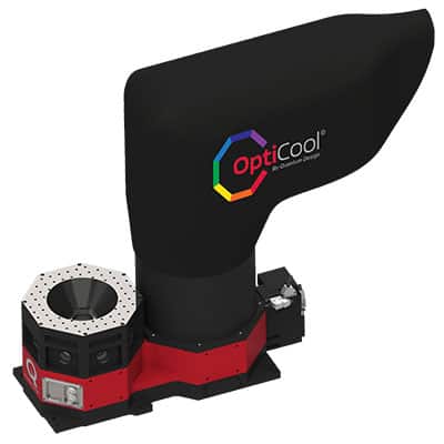
The result? A unique, award-winning magneto-optical cryostat that offers researchers a much larger sample space, unrivalled optical access, and the ability to probe materials at temperatures below 2 K and magnetic fields as high as 7 T. Typical experiments might include optical inspection of a sample using a high-performance microscope objective, or pump−probe experiments that exploit pulses of light to analyse the behaviour and dynamics of materials at different temperatures and magnetic fields.
The OptiCool provides full control over the temperature and magnetic field so that researchers can study their sample in any environment.
Randy Black
“The OptiCool provides full control over the temperature and magnetic field so that researchers can study their sample in any environment,” says Q-Works team member Randy Black. “It’s also designed with lots of windows to get light in and out of the cryostat in a very efficient and convenient way.”
Innovative design: The OptiCool instrument has been designed to be integrated into an optical table, and allows the sample can be positioned right inside the coils of the superconducting magnet. (Courtesy: Quantum Design)
The reimagined design allows the cryostat to be integrated into an optical table, rather than needing the whole experiment to be assembled inside a separate cryostat. Seven side ports provide optical access of 270° around the sample, with an extra window allowing light in from the top. The cryostat can even be mounted on legs to allow light to enter and exit the instrument from underneath. “We wanted to create a system where the user has much better access to their sample in the optical environment,” says Neils.
According to Neils, the design of commercial magneto-optical cryostats has largely stood still for the last 30 years. With no dedicated optical cryostat in Quantum Design’s product line-up, and growing interest among the research community in using light-based measurement techniques at low temperatures, the Q-Works team saw an opportunity to create something new.
When the three physicists surveyed the competition, they found that none of the existing magneto-optical cryostats offered the perfect combination of features. High on the list of requirements is cryogen-free cooling that avoids the need for liquid helium, but these “dry” cryostats generate vibrations that can perturb precise optical measurements. To minimize these unwanted vibrations, existing instruments either revert to cooling with liquid helium or do not provide the option for a magnetic field. “We decided to create a product that no-one else was making: one that combined low vibrations, high magnetic field and cryogen-free cooling,” comments Black.
At the heart of the design is a unique geometry that moves the cryogenic components away from the sample. “We’ve created this kind of castle, an octagonal region where the magnet and the sample live, and pushed the cooler off to the side, out of the way,” explains Neils. “It’s a very open design, and means that the sample isn’t buried inside a large cryostat away from the optics.”
It’s a very open design, and means that the sample isn’t buried inside a large cryostat away from the optics.
William Neils
A crucial element of this approach is a split-coil, conical magnet designed and built by the Q-Works team. With a large bore size – almost 100 mm across – the sample can be positioned right inside the magnet, which is capable of generating magnetic fields of ±7 T. “In normal split-pair magnets, all the optical components have to be far away from the sample because the magnet is in the way,” says Dinesh Martien, the third Q-Works team member. “The conical shape allows you to bring your optical components much closer to the sample.”
The Q-Works physicists knew right from the start that they would need to design the superconducting magnet themselves. “Normally we would buy the magnet from another supplier, but we wanted to use every bit of space as efficiently as possible,” says Black. “It’s a very tight fit, with clearances of just a millimetre between surfaces and around the magnet, and we figured that we would have real problems if we tried to outsource that part of the design.”
While the team needed to learn how to build a superconducting magnet, they were also keen to exploit technologies they had already developed for Quantum Design’s broader product portfolio of high-performance cryostats. Much of the electronics used for temperature control, for example, was lifted from the Physical Property Measurement System (PPMS) DynaCool, as well as some of the operating software and the mechanisms for magnet control. That pragmatic approach allowed the team to invent and launch a completely new instrument within just three years, with the first products being installed in research labs by early 2019.
Previous experience with cryostat systems also inspired an early decision to design a modular system for loading the sample into the cryostat. Most refrigerators require the user to connect all the wiring inside the instrument, which makes it difficult to reach all the experimental components and connections. For the PPMS DynaCool system, however, the sample is loaded on to a small puck 25 mm across and then lowered into the instrument to make the measurement.
It’s really convenient for the user to be able to mount their sample and connect the wires to it while it’s on the bench.
Dinesh Martien
“It’s really convenient for the user to be able to mount their sample and connect the wires to it while it’s on the bench,” says Martien. “We needed to develop something that would fit into the geometry we had, and that would cope with a lot of wiring, as well as different types of wiring, to cope with things like piezoelectric nanopositioners and high-frequency radio signals.”
In a moment of serendipity, the Q-Works team realized that their bespoke magnet design would make it possible to create a much larger sample holder. “We hadn’t thought too much about that modularity until midway into the project, at which point we were also having difficulty with the magnet,” recalls Black. “We realized that making the magnet bigger would reduce the stresses in the system, and then the large bore size would provide a huge amount of space for a puck-like sample holder – which we then decided to call a sample pod.”
The team has now shipped a number of OptiCool instruments to academic labs in North America, Europe, and Asia, and the novel design was recognized by R&D World as one of the most innovative products introduced in 2018. The first instrument was installed in the lab of regular collaborator Richard Averitt at the University of California San Diego, who has been using it for pump–probe experiments with gadolinium titanate, a material that becomes magnetic when light is shined on it. “Integrating the OptiCool into my research program will make it possible to access an experimental phase space in complex materials that simply wasn’t available to my group in the past,” Averitt comments.
Just the job: how the sample can sit inside the magnet (Courtesy: Quantum Design)
Neils says that research scientists have been excited about the experimental possibilities opened up by the OptiCool cryostat, even though it can take a while for them to work out how they can use it most effectively. “It’s different enough that it doesn’t fit into a category that they already know, so they often come back to us with questions,” he says. “Typically the scientists will look at the instrument, get an idea of how it can help, and then they will apply for a research grant to enable them to place an order.”
As well as time-resolved pump–probe experiments, researchers are using the instrument for free-space optics, or for imaging the surface of the sample using an optical microscope. Some research groups are interested in diamond-anvil cells, in which case optical access offers a mechanism for measuring the pressure inside the cell, while others are focusing on high-frequency signals using coaxial lines.
But it’s still too soon even for the early adopters to publish new research results based on experimental data obtained with the OptiCool. In the meantime, the Q-Works team is refining the instrument and building pre-configured options for some of the most common experimental requirements, such as nanopositioners, microscope objectives, and coaxial lines. “We’re not looking at turnkey measurements yet,” says Martien. “But we are aiming to integrate a microscope objective into the instrument, with nanopositioners below it, which would enable users to image their sample over a 2D region.”
The early success with the OptiCool instrument has also secured the future of the Q-Works programme for at least another year. “We’re going to continue to support this product, while also keeping an eye out for other ideas,” says Neils. “Hopefully we will have another winner.”
Q-Works: a new way to innovate
In early 2015, seeking to expand outside its traditional markets, Quantum Design’s directors charged William Neils with creating a dedicated R&D unit to identify and deliver a new business opportunity for the company. “The owners realized that they needed a different way to generate new product ideas, so they decided to pull a small group of people away from the normal day-to-day routine,” says Neils. “I immediately went to Randy [Black] and Dinesh [Martien] because we had worked closely together on a previous project and we worked very well together.”
The three physicists moved out of the main company building and set themselves up in a nearby suite. Apart from needing to find out how to procure essential services such as technical equipment and a regular supply of coffee, the team relished the freedom and the challenge of working outside the main company. “The suite was our own little sandbox to play in,” says Neils. “It felt like the company was expecting great things, and we knew it was important to rise to the challenge.”
The winning formula for the Q-Works physicists was to invent a completely new instrument that also exploited their existing knowledge of cryogenics systems. “We knew we were getting a lot of eyes on us,” says Martien. “When we evaluated what we should develop, we decided to produce a product that would enable us to leverage existing technologies so we could create something more quickly.”
With a successful product on the market within three years of setting up Q-Works, it seems that the gamble has paid off. “This was really a time when the whole company came together to implement and roll out the product,” says Barak Green, Quantum Design’s marketing manager. “It’s one of those success stories where everyone can feel good about what we’ve achieved.”





 Imagine a perfect diamond lattice of repeating carbon atoms. Remove two adjacent atoms, then replace one with nitrogen (bright blue in figure), while the other remains a “void” or vacancy (pale blue). This is the neutral nitrogen-vacancy defect in diamond, and it can have four different crystallographic orientations. Should there be another defect nearby in the lattice that has an electron with higher energy – usually a substitutional nitrogen that has no vacancy – this electron will transfer to the nitrogen-vacancy to give it a negative charge.