Japanese researchers are closing in on understanding why electrical storms have a positive influence on the growth of some fungi. In a series of experiments, Koichi Takaki at Iwate University and colleagues showed that artificial lightning strikes do not have to directly strike shiitake mushroom cultivation beds to promote growth. Now they are developing technology to use electric stimulation in the production of the mushrooms, which are popular in many east Asian cuisines.
Bizarre as it may seem, atmospheric electricity has long been known to boost the growth of living things, including plants, insects and rats. In 1775, the priest and physicist Giovanni Battista Beccaria of the University of Turin reported, “it appears manifest that nature makes extensive use of atmospheric electricity for promoting vegetation”.
David Graves at the University of California at Berkeley, an expert on plasmas in food and agriculture who was not involved in this mushroom study, said “Historically, most people who looked at it [atmospheric electricity] systematically found some effect, but it can sometimes be hard to reproduce, so it’s still not by any means fully accepted in the community and there’s little understanding of the mechanism.” However, at recent plasma conferences, Graves was favourably impressed by the results presented by Takaki.
Fruiting bodies
Takaki explains, “We use high voltage electric shock as stimulation to change the mushroom growth state from vegetative to reproductive growth of fruiting bodies”. Takaki, is an expert on discharge plasma and high voltage engineering and aims to improve the cultivation shiitake mushrooms in countries that suffer from low yields.
Shiitake mushrooms are grown in hardwood logs in a process that takes one year. First, branching vegetative filaments called hyphae are grown in the logs, which are kept in beds. Farmers then submerge the logs in water for 1-2 days and then beat the logs mechanically. When this is done skilfully, it disrupts the interlinking hyphae, moving the shiitake into its reproductive phase of growth that produces the desirable mushroom caps.
In Takaki’s previous studies, yield increases were achieved by running a direct current through a shiitake mushroom log. But Takaki still wondered – why do natural electric storms indirectly influenced the growth of mushrooms located miles away from the lightning strikes?
Other physical events
He hypothesized that it was not purely high-voltage electricity stimulating mushroom growth, but that other physical events must be triggered and ripple out into the surrounding environment. To test this, Takaki’s team investigated the effects of more natural, indirect strikes on growth.
They took logs ready for stimulation, performed a 24 h submersion in water, and then arranged the logs 3 m offset from the lower and upper electrodes of an impulse voltage generator. In an electrical storm a cloud generates 3-4 strikes on average, so the team programmed the same number of sparks to sequentially discharge between electrodes.
That was day one. The team harvested mushroom caps more than 50 mm in diameter on days 9, 11 and 13, recording fruiting body number and size. They collected approximately twice as many mushrooms on logs exposed to lightning strikes 3 m away, compared to mushrooms produced by the control set of logs sitting 12 m away within the same facility.
A third set of logs were exposed to daily sets of lightning strikes for a week and they produced an even higher yield than those only exposed to one set of strikes.
A shock to the system
“The large current from a lightning strike causes temperature to quickly rise from room temperature to about 10,000 °C,” explains Takaki. “This quick rise in temperature rapidly increases the volume of the air producing a shock wave that propagates to, and then vibrates inside the log. This moves the hyphae inside the log, breaking the strands and stimulating fruiting body formation.”
Current mechanical stimulation methods create pressure waves only partially infiltrating the logs. “Lightning produces a shock wave that propagates homogenously, so it can cut many parts of the hyphae in a controllable manner,” said Takaki.
The team are working to adapt their equipment for deployment in the fungiculture industry. To find a more practical approach, Takaki’s students tried to simulate shock waves using sound from a speaker. However, from preliminary experiments, Takaki does not think the sound is loud enough to emulate the intense pressure waves generated by a lightning strike.
“We are trying to develop a cheap and compact machine so many people, not only in Japan, but also in Thailand, India and Nepal can use our technology,” said Takaki.
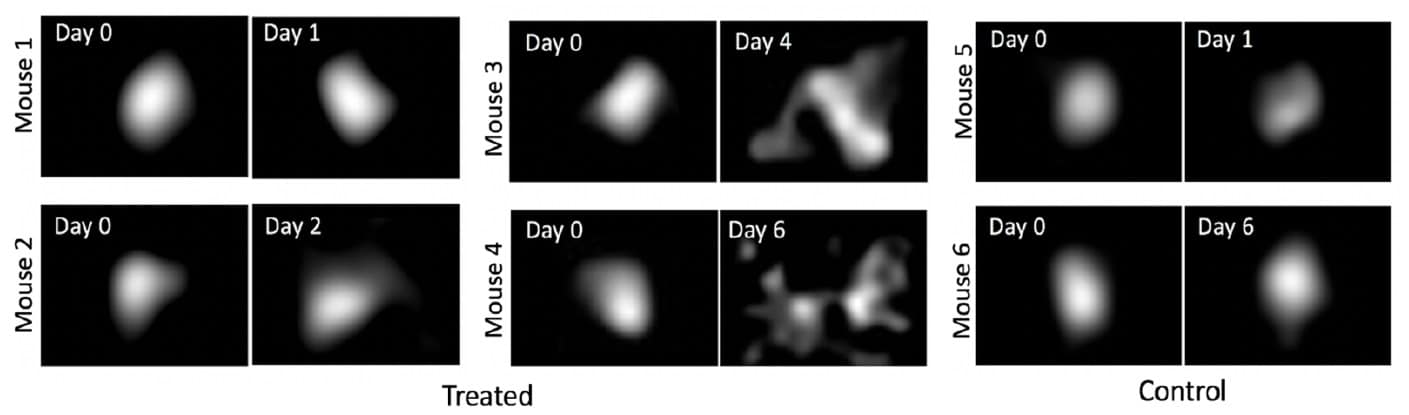
Cherenkov-excited luminescence images of phosphorescent ink in four treated mice (1–4) and two control mice (5 and 6). (Courtesy: Phys. Med. Biol. 10.1088/1361-6560/ab7d16)
Monitoring tumour progression during a course of radiation therapy can help determine whether a treatment is working or not. Such tracking is mostly anatomy-based, using weekly CT scans, for example, to measure tumour size. This approach, however, can fail to detect subtle changes at the cellular level – a task that calls for functional imaging.
Functional imaging modalities can characterize responses of the tumour microenvironment. But common techniques, such as PET or diffusion-weighted MRI, require a separate scheduled exam. Researchers from Dartmouth College’s Thayer School of Engineering have now proposed a way to image the tumour microenvironment during radiotherapy without interrupting the clinical workflow, using Cherenkov-excited luminescence imaging (CELI). They achieve this by employing CELI to track the spread of a phosphorescent tattoo ink (Phys. Med. Biol. 10.1088/1361-6560/ab7d16)
CELI works by using the Cherenkov light generated as the treatment beam travels through tissue to excite a luminescent agent – in this case, a UV-sensitive tattoo dye injected into the tumour. The researchers propose that as tumour cells break down in response to irradiation, the dye will spread. This diffusion can then be measured during radiotherapy by using a camera to image the emitted phosphorescence signals.
“In the last few years, our lab has done a great deal of radiotherapy research focused on imaging the radiation beam delivered to the patient in real time using time-gated Cherenkov imaging,” says first author Jennifer Soter, a PhD student in Brian Pogue’s research group. “We were prompted to expand on this technology further and explore additional applications in cancer treatment. In the case of tumour progression in radiotherapy, there’s really no feasible method that enables daily imaging of tumours clinically.”
In vivo investigations
Soter and colleagues used a mouse model to evaluate whether CELI can directly track subtle changes in the tumour microenvironmental in response to radiation therapy. On day zero, they injected tattoo ink into the centre of tumours in 20 mice. They then delivered a 1.4 Gy treatment fraction to all mice, using 6 MV X-ray beams from a clinical linac, and performed a baseline CELI session to measure the initial spread of the ink.
The researchers used an intensified CMOS camera to detect visible phosphorescence from the ink. The camera was time-gated with the linac pulses, such that it only recorded the delayed phosphorescence signals emitted between each radiation pulse. Immediately after the first CELI session, they delivered an additional 12 Gy dose to 15 mice, while nine untreated controls received no additional radiation. One to six days later, they delivered a second 1.4 Gy to each mouse and performed the final CELI session
By comparing images acquired immediately after injection with the final diffusive ink spread, the researchers could determine the tumour response. “Cell death via apoptosis and necrosis can lead to significant sections of the tumour decreasing, resulting in tissue clearance, which is well known from diffusion MRI,” explains Soter. “The ink is a simple label that also diffuses from within the tumour as the pressure decreases.”
In the control group, ink distributions remained constant after four days, with less than 2% diffusive spread. In treated mice, on the other hand, the ink spread reached almost 200% by day six. From two days post-injection, the team could see a significant difference in diffusive spread values between treated mice and control mice.
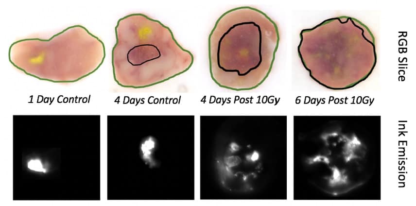
Following the final CELI session, the researchers euthanized the mice and imaged tumours using hyperspectral cryo-fluorescence imaging to quantify radiation-induced necrosis. Different regions of tumour – the non-perfusing necrotic core, the viable tissue and the dye – exhibited clearly different reflectance spectra.
Non-perfusing necrotic core (black outline) in tumour slices tissue and corresponding fluorescence images from the ink. (Courtesy: Phys. Med. Biol. 10.1088/1361-6560/ab7d16)
The ex vivo analysis confirmed the trends seen with in vivo CELI. As the volume of necrotic core increased, the fluorescence image slices showed increasing ink diffusion. Analysing the in vivo ink spread revealed a strong correlation with the percentage of necrotic volume, but a weak correlation with total tumour volume (measured manually with callipers).
The researchers conclude that the spread of injected tattoo ink can be related to radiation-induced necrosis, independent of total tumour volume change. They propose that this in vivo imaging system offers potential to track treatment response daily, without interrupting clinical workflow.
They note that translating this approach to the clinic will require further developments. These include: increasing in vivo image resolution by moving from widefield irradiation to sheet-scanning illumination; developing a phosphorescent tattoo ink that’s safe for humans; and investigating the effects of injection site to account for inherent tumour heterogeneity.
“Next, we plan to perform more studies of immune infiltration as related to the change in ink diffusion, as well as studies of different types of tumours with variations in stromal density and radiosensitivity,” Soter tells Physics World.
Ions trapped nanoscale optical cavities could be used to distribute entangled quantum particles over large distances. That is the conclusion of Jonathan Kindem and colleagues at Caltech in the US, who showed that a trapped ion of ytterbium can remain entangled with a photon for long periods of time. Furthermore, the team showed that the ion’s quantum state can be read out when manipulated by laser and microwave pulses. Their achievement could lay the foundations for a future quantum internet.
Quantum computers are becoming a reality as research labs and companies roll out nascent devices. An important next step in this quantum revolution is creating a “quantum internet” across which quantum information can be shared. The delicate nature of quantum information, however, means that it is very difficult to connect quantum computers over long distances.
Most quantum computers encode quantum bits (qubits) of information into the quantum states of matter – trapped atoms or superconducting circuits, for example. However, the best way to transmit quantum information over long distances is to encode it into a photon of light. An important challenge is how to transfer quantum information from stationary matter-based qubits to photon-based “flying” qubits and then back again.
Attractive properties
Qubits made from solid materials interact strongly with light and therefore readily transfer quantum information to photons. However, these qubits tend to be very short-lived, which makes it difficult to use them to build practical quantum computers. Trapped atoms or ions, on the other hand, can make long-lived qubits but interact weakly with light. Rare-earth ions have properties that could make them particularly long-lived qubits, but physicists have struggled to trap them in such a way that they can be controlled and interact with light.
In their study, Kindem’s team showed that this problem could be overcome by placing a rare-earth ion of ytterbium in an optical cavity to enhance its interaction with light. To do this, they fabricated a periodic, nano-patterned 10 micron-long cavity with the ion at its centre. Light bounces back and forth many times in the cavity, greatly increasing the chance of the light interacting with the ion.
The researchers then manipulated their ion qubit using laser and microwave pulses. The result is the emission of a photon that is entangled with the qubit – a photon that itself is a flying qubit of quantum information.
More than 99% of the time, they found that this entangled photon remained inside the cavity, bouncing back and forth. This allowed the team to study the photon-ion system over a relatively long time period. Indeed, Kindem and colleagues observed that the photon and ion can remain entangled for up to 30 ms – long enough for the photon to travel across the continental US.
Kindem’s team now hopes to scale up their experiment to enable information exchange between two real, distant qubits — demonstrating the building blocks of a realistic quantum internet. Within such a network, quantum computers in widely spaced geographical locations could share data and perform calculations together; potentially allowing extremely large computations to take place. It could also enhance the prospects for quantum cryptography by allowing networks of trusted parties to exchange information securely using entangled particles.
Researchers in Israel have made a new type of contact lens that can correct a form of red–green colour blindness known as deuteranomaly. By incorporating plasmonic metasurfaces into standard contact lenses, the researchers were able to restore lost colour contrast and improve colour perception by up to a factor of 10.
Humans can typically distinguish more than a million colours, but for some, colour perception is limited in certain ranges of the electromagnetic spectrum. In these individuals, the response of the light-sensitive cone photoreceptor cells at the back of the eye is attenuated when excited with a specific wavelength of light.
In deuteranomaly, for example, signals from the cells that are sensitive to green–yellow light (known as medium-type cone photoreceptors) are dulled. This means that the brain receives too many signals from longer wavelengths associated with yellow–red light. The result is that people with this form of colour blindness struggle to tell red and green wavelengths apart. Although special glasses that reduce perception of yellow–red light are available, they are bulky and uncomfortable to wear.
Artificially-engineered thin metallic films
Researchers Sharon Karepov and Tal Ellenbogen from Tel Aviv University, have now transferred metasurfaces – artificially engineered thin metallic films that can be fine-tuned to interact with light in very specific ways – onto the surface of commercially available contact lens to achieve the same filtering capability.
The metasurfaces work by exploiting the physics of plasmons, which are quasiparticles that arise when light interacts with the electrons in a metal and makes them oscillate. The shape, size and arrangement of the nanoscale structures – in this case, a 40-nm-thin film of nanosized gold ellipses – within plasmonic materials makes it possible to support plasmons at specific frequencies. By thus adjusting these structural parameters, the researchers can control which frequencies of light the material will absorb and scatter.
From flat to curved surfaces
Since metasurfaces are usually fabricated on flat surfaces, Karepov and Ellenbogen needed to develop a technique to transfer them onto the curved surface of a contact lens. Their new fabrication process opens the door for embedding these materials into other non-flat substrates as well, they say.
By testing the optical response of the metasurface at every stage of the new fabrication technique and imaging its structure, the researchers confirmed that its light manipulation properties did not change after transfer to the curved surface.
Factor of 10 improvement in colour perception
They then simulated how a wearer of their new nanostructured contact lens would perceive colour using standard tests based on Commission International de l’Eclairage (CIE) colour spaces and conventional models of human colour-sensitive photoreceptors. They found that the device could shift incorrectly recognized colours closer to the original hues and that lost visual contrast in red–green colour blindness could essentially be restored (see image). Indeed, they measured an improvement of up to factor of 10 in colour perception. An Ishihara-based colour-blindness test (the most well known colour perception test for red–green colour deficiencies) also confirmed contrast restoration.
While the new lens still needs to pass clinical-stage tests, the researchers say that manufacturers could potentially embed the metasurfaces during the moulding stage of contact lens fabrication or thermally fuse them to a rigid lens. They plan to continue improving their metasurface transfer process and test it for other applications too.
Graphite films can shield electronic devices from electromagnetic (EM) radiation, but current techniques for manufacturing them take several hours and require processing temperatures of around 3000 °C. A team of researchers from the Shenyang National Laboratory for Materials Science at the Chinese Academy of Sciences has now demonstrated an alternative way of making high-quality graphite films in just a few seconds by quenching hot strips of nickel foil in ethanol. The growth rate for these films is more than two orders of magnitude higher than in existing methods, and the films’ electrical conductivity and mechanical strength are on par with those of films made using chemical vapour deposition (CVD).
All electronic devices produce some EM radiation. As devices become ever smaller and operate at higher and higher frequencies, the potential for electromagnetic interference (EMI) grows, and can adversely affect the performance of the device as well as that of nearby electronic systems.
Graphite, an allotrope of carbon built from layers of graphene held together by van der Waals forces, has a number of remarkable electrical, thermal and mechanical properties that make it an effective shield against EMI. However, it needs to be in the form of a very thin film for it to have a high electrical conductivity, which is important for practical EMI applications because it means that the material can reflect and absorb EM waves as they interact with the charge carriers inside it.
At present, the main ways of making graphite film involve either high-temperature pyrolysis of aromatic polymers or stacking up graphene (GO) oxide or graphene nanosheets layer by layer. Both processes require high temperatures of around 3000 °C and processing times of an hour. In CVD, the required temperatures are lower (between 700 to 1300 °C), but it takes a few hours to make nanometre-thick films, even in vacuum.
High-performance films
A team led by Wencai Ren has now produced high-quality graphite film tens of nanometres thick within a few seconds by heating nickel foil to 1200 °C in an argon atmosphere and then rapidly immersing this foil in ethanol at 0 °C. The carbon atoms produced from the decomposition of ethanol diffuse and dissolve into the nickel thanks to the metal’s high carbon solubility (0.4 wt% at 1200 °C). Because this carbon solubility greatly decreases at low temperature, the carbon atoms subsequently segregate and precipitate from the nickel surface during quenching, producing a thick graphite film. The researchers report that the excellent catalytic activity of nickel also aids the formation of highly crystalline graphite.
Using a combination of high-resolution transmission microscopy, X-ray diffraction and Raman spectroscopy, Ren and colleagues found that the graphite they produced was highly crystalline over large areas, well layered and contained no visible defects. The electron conductivity of the film was as high as 2.6 x 10⁵ S/m, similar to films grown by CVD or high-temperature techniques and pressing of GO/graphene films.
To test how well the material could block EM radiation, the team transferred films with a surface area of 600 mm2 onto substrates made of polyethylene terephthalate (PET). They then measured the film’s EMI shielding effectiveness (SE) in the X-band frequency range, between 8.2 and 12.4 GHz. They found an EMI SE of more than 14.92 dB for a film approximately 77 nm thick. This value increases to more than 20 dB (the minimum value required for commercial applications) in the entire X-band when they stacked more films together. Indeed, a film containing five pieces of stacked graphite films (around 385 nm thick in total) has an EMI SE of around 28 dB, which means that the material can block 99.84% of incident radiation. Overall, the team measured an EMI shielding of 481,000 dB/cm2/g across the X-band, outperforming all previously reported synthetic materials.
Thinnest among reported shielding materials
The researchers say that to the best of their knowledge, their graphite film is the thinnest among reported shielding materials, with an EMI shielding performance that can satisfy the requirement for commercial applications. Its mechanical properties are also favourable. The material’s fracture strength of roughly 110 MPa (extracted from stress–strain curves of the material placed on a polycarbonate support) is higher than that of graphite films grown by the other methods. The film is flexible, too, and can be bent 1000 times with a bending radius of 5 mm without losing its EMI shielding properties. It is also thermally stable up to 550 °C. The team believes that these and other properties mean that it could be used as an ultrathin, lightweight, flexible and effective EMI shielding material for applications in many areas, including aerospace as well as electronics and optoelectronics.
Just for fun, here are 10 physics trivia questions to provide some amusement during the global lockdown and to test your knowledge of physics past and present. Don’t worry, you don’t need to calculate anything or know any physics either.
1 What was Brian Cox’s role in the band D:REAM, which had a hit in the 1990s with Things Can Only Get Better? A Vocals B Drums C Keyboards D Guitar
2 Which activity did madcap German theoretical physicist Theodor Kaluza successfully do for the first time after only ever having studied it in a book? A Chess B Swimming C Knitting D Yoga
3 Where did pioneering physicist James Joule carry out his early experiments on thermodynamics? A In a brewery B On a farm C In a river D In his bedroom
4 What has animal-loving Queen guitarist and former astrophysicist Brian May got in his garden? A Satellite dish B Physics lab C Cat sanctuary D Telescope
5 What pet belonging to top Scottish physicist James Clerk Maxwell appears on his statue in Edinburgh? A Cat B Hamster C Dog D Budgie
6 When Isaac Newton died, which of these was not in his possession? A Cheese toaster B Brown teapot C Mohair bed D Shower curtain
7 In TV’s The Big Bang Theory, Leonard, Raj, Howard and Sheldon are researchers at which US institution? A Caltech B Berkeley C Stanford D UCLA
8 Physicists Sabine Hossenfelder and Tim Palmer recently recorded a spoof coronavirus version of which song? A Stayin’ Alive – The Bee Gees B Sick and Tired – The Cardigans C It’s the End of the World as we Know It – REM D Heaven Knows I’m Miserable Now – The Smiths
9 Who has never appeared in the Physics World “Once a Physicist” column (which features people who once studied physics)?A Olympic canoeist B Opera singer C Prize-winning poker player D Professional footballer
10 Which US institution once offered a professorship to the Italian scientist Galileo Galilei? A College of William and Mary B Harvard University C Penn State University D Yale University
Stuck on any questions? We’ll reveal the answers on the next episode of the Physics World Weekly podcast on Thursday 16 April and on this blog on Friday 17 April. In the meantime, you can see what the rest of the world thinks by checking our online polls at #physicsCoronavirusQuiz on Twitter.
Update: Answers: 1 C 2 B 3 B 4 D 5 C 6 D 7 A 8 C 9 D 10 B (although we’re not entirely sure about that last one any more!)
Recent developments in 3D printing of metallic biomaterials enable fabrication of orthopaedic implants tailored for bone reconstruction following trauma or bone tumours, or for use in joint replacements, spinal implants and reconstructive surgery. It’s also possible to fabricate these implants with surface properties that can promote bone-tissue regeneration and minimize the risk of implant-associated infections.
Insertion of any implant in the human body, however, triggers an immune response that can influence the above-mentioned biofunctionalities.
Aiming to minimize the risk of implant-associated infections, a multidisciplinary research team from the Netherlands involving engineers from TU Delft and biologists from Erasmus MC has examined the in vitro immune response triggered by porous titanium implants printed using selective laser melting (SLM). The team examined three types of SLM implants: untreated; surface biofunctionalized using plasma electrolytic oxidation (PEO); and PEO-biofunctionalized in the presence of silver nanoparticles (PEO+Ag) to provide antibacterial functionality (Biomed. Mater. 10.1088/1748-605X/ab7763).
“Most of the research on implants is focused on how they can stimulate formation of the new tissue, with very scarce data on the inflammatory response they elicit,” explains Lidy Fratila-Apachitei from Delft University of Technology. “Our implants are designed to stimulate bone regeneration and prevent implant associated infections. The inflammatory responses triggered by these implants may affect both these biofunctionalities. Therefore, we were interested to know how inflammatory cells (macrophages) respond to our implants.”
In vitro behaviour
Implanted biomaterials trigger responses that activate both pro-inflammatory and anti-inflammatory, pro-healing macrophages. The fine balance between these two types is influenced by the biomaterial’s properties. To investigate this, the researchers examined the response of human peripheral blood monocyte-derived macrophages cultured on the three different titanium implants.
The untreated implants triggered a strong pro-inflammatory response in macrophages, including relatively high levels of genes that may have detrimental effects on healing, combined with early anti-inflammatory effects. PEO-treated implants showed a higher potential to induce pro-healing macrophages, while incorporation of silver nanoparticles led to cytotoxic effects.
Cell type matters
The team also examined the culture of human mesenchymal stromal cells on the same implants and observed that they survived on all surfaces. This finding indicates that the PEO+Ag implants were not cytotoxic for these cells, in agreement with previous research, and suggests different levels of silver toxicity for different cell types.
The researchers emphasize that macrophage sensitivity to the presence of silver nanoparticles may lead to a compromised immune response in vivo. Therefore, the team is working on finding the optimum concentration of silver nanoparticles that would ensure both macrophage viability and antibacterial function of the implant. Thereafter, the researchers will continue to explore the immunomodulatory effects observed with the aim of achieving immune responses that may favour bone regeneration.
In 2018 the nanotechnology community was wowed by two breakthroughs in graphene research made by a team led by Pablo Jarillo-Herrero of the Massachusetts Institute of Technology (MIT) in the US. Their discoveries led to the rapid emergence of a field called twistronics, which offers a new and very promising technique for adjusting the electronic properties of graphene by rotating adjacent layers of the material.
Calling graphene a wonder material may sound trite, but it is an eminently suitable moniker for a material that continues to amaze condensed-matter physicists like Jarillo-Herrero. I chatted with him about what has happened since his team revealed in 2018 that magic-angle graphene is both a high-temperature superconductor and a Mott insulator.
Graphene is a free-standing sheet of carbon just one atom thick that was first isolated in 2004 by Andre Geim and Konstantin Novoselov – earning the University of Manchester duo the 2010 Nobel Prize for Physics. Since then, researchers have shown that the material has a range of notable and potentially useful properties ranging from high-electron mobility to great physical strength.
Layers of graphene stack upon each other to make the familiar material graphite. Twisted graphene can be made from two sheets of graphene by rotating the sheets away from the usual stacking angle.
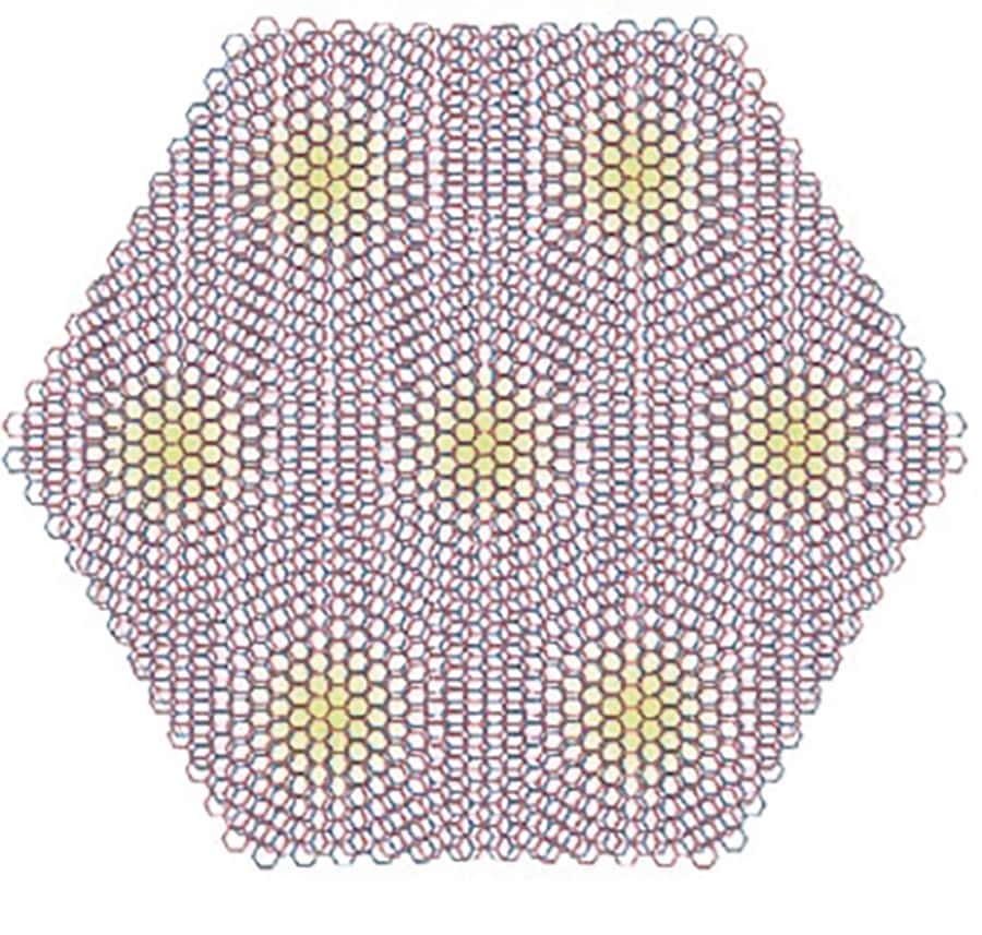
Jarillo-Herrero has been working on twisted graphene since 2009. But the big breakthrough came in 2018, when his team reported how it had stacked two sheets of graphene on top of each other and then twisted the sheets so that the angle between them was 1.1°. At this theoretically predicted “magic angle”, the researchers had expected to observe a range of interesting physics. This is because carbon atoms in the two overlapping graphene crystals create a moiré superlattice.
They were not disappointed and made two very important discoveries. First, they found that magic-angle graphene is a Mott insulator. This is a material that should be a metal but is instead an insulator because of strong interactions (correlations) between electrons.
Then, they added a few extra charge carriers to this Mott-insulator state by applying a small electric field, which turned magic-angle graphene into a superconductor at temperatures below 1.7 K. Despite the low temperature, the proximity to the Mott insulator state and low electron density of the material mean that the material resembles a high-temperature superconductor. So, with a simple twist, Jarillo-Herrero’s team had created a system where small adjustments in terms of angle and electric field creates two iconic states of condensed matter physics – a Mott insulator and a high-temperature superconductor.
It has only been two years since Jarillo-Herrero’s team described its results in two papers, and the work has been cited more than 1200 times. He says that most of the citations are from theorists and that there are now hundreds of theory groups working on the system. It takes longer for experimentalists to learn how to make and characterize magic-angle graphene, but Jarillo-Herrero reckons that there are about 20–25 experimental groups that already have results on the material.
Our discovery is the tip of the iceberg, there is so much more underneath
Pablo Jarillo-Herrero
Despite this huge effort, the physics of magic-angle graphene is still in its infancy and Jarillo-Herrero says that there are many things to study. Beyond superconductivity and the strongly correlated states – both of which occur at low temperatures – he says that there is much to learn about the material at higher temperatures.
He is also keen to study other 2D materials that can be twisted. One possibility is bilayer graphene on top of bilayer graphene with a twist between the two bilayers. Twisted bilayers are expected to have interesting correlated-electron physics with magnetic properties that are different to those of the original twisted graphene.
Jarillo-Herrero’s team is also looking at twisting materials unrelated to graphene such as 2D superconductors and 2D magnets. There are theoretical predictions, for example, that a special kind of magnetism called moiré magnetism occurs when 2D magnets are twisted on top of each other.
Moiré patterns Magic angle graphene superlattice. (Courtesy: P Jarillo-Herrero)
“Our discovery is the tip of the iceberg, there is so much more underneath,” he says, “There is a lot of work for many years to come”.
Jarillo-Herrero is frank and honest about the technological applications of magic-angle materials. “Don’t expect any applications in for 30–40 years – which is the normal timescale for a new material.”
He believes that one technology that could emerge is a superconducting transistor that can be switched between superconducting and normal states. Such devices could be used in cryogenic classical computers, which would run at very low temperatures to avoid the power dissipation problems associated with high-speed silicon processors. Other options include using twisted materials to make superconducting single-photon detectors or superconducting quantum bits for quantum computing.
However, he points out that the technology is still in its infancy in terms of making large and consistent samples of twisted materials.
In the nearer future, Jarillo-Herrero says that magic-angle materials have a wide range of fascinating physics that will be explored. One avenue is quantum simulation, whereby twisted graphene is used as a proxy for a more complicated material such as a high-temperature superconductor.
And, of course, he points out that there should be lots of interesting physics – including topological properties – lurking in twisted graphene itself, which will keep researchers busy for years to come.
Cities and countries worldwide are working towards being net carbon neutral. In this episode of the Physics World Weekly podcast the science journalist Kate Ravilious talks to about some of the ways that people and governments are trying to achieve this goal.
Linear accelerators (linacs) for treating cancer are among the most complicated technologies used in hospitals. As well as being difficult to operate, mistakes cause damage to a linac or leave it in a state in which it could do harm to patients. Training new medical physicists in how to use linacs is difficult, however, because the machines are normally in use treating patients. In this episode, Physics World’s Tami Freeman talks to Marco Carlone in Canada, who has founded a company called Linax Technologies to develop a linac simulator that could be used for training purposes.
Finally Margaret Harris and Hamish Johnston talk about space-weather super-storms and how they can damage electrical grids. They also explain how a new map from the US Geological Survey identifies power lines in the US that are most vulnerable to super-storms.
For some science students, the path from undergraduate degree to career of choice is a linear and seemingly friction-free transition. For others, less so. Stephanie Mottershead, a project manager at Surrey Satellite Technology Ltd (SSTL), a UK manufacturer of small satellite systems, definitely falls into the second category. After completing a BSc in geology and environmental science at the University of Bristol, Mottershead walked straight into a tanking graduate jobs market and a wider economy reeling from the aftershocks of the 2008 financial crash.
Needs must, though, and Mottershead spent the next decade or so on a very different career trajectory, working as a professional singer in London and on various luxury cruise ships. Her passion for science undimmed, she also managed to study part-time for an Open University (OU) degree in physics and astronomy. “I loved the planetary-science modules in my OU course and it gradually dawned on me that I could do something with this professionally,” she explains. “Rather than continue with music as a career and science as a hobby, I made the decision to switch things around.”
Mottershead’s reinvention took off in 2017 when she secured a European Space Agency (ESA) scholarship to attend the International Space University’s Space Studies Program in Cork, Ireland. This nine-week residential “summer space camp” brings together around 250 delegates each year, among them early-career scientists and engineers intent on forging a path in the space industry alongside established professionals seeking to broaden their knowledge of the space sector beyond their current discipline. “The Space Studies Program was an incredible experience,” says Mottershead. “To meet and learn from a network of experts and peers like that really opened my eyes to the range of career paths available within the space industry.”
Own the space
Spurred on by her experience in Cork, Mottershead wrapped up her OU degree in double-quick time and set her sights on UCL’s MSc in space science and engineering. “The 12-month programme at UCL aligned with my desire to combine planetary science and space engineering,” she says. “I wanted to pursue both and the mix of taught-course modules ties everything together really well.”
Stephanie Mottershead: “The MSc is the most intense thing I’ve ever done, but massively rewarding at the same time.” (Courtesy: Stephanie Mottershead)
Another factor in Mottershead’s choice of UCL is the reputation of the teaching and research staff. “You get to learn from world-leading experts in all fields of space science,” she explains. “For our individual research projects, we also got to work with scientists and engineers at UCL’s Mullard Space Science Laboratory (MSSL) – all of whom are actively involved on high-profile space missions like the recently launched Solar Orbiter (see box, below).”
The taught element of the MSc course, which takes up the first six months of the programme, is followed by an individual research project and dissertation, a group research project (involving the full MSc cohort), plus exams for good measure. “There’s no let up at all,” adds Mottershead. “It’s the most intense thing I’ve ever done, but massively rewarding at the same time.”
In terms of specifics, the lecture programme comprises a series of compulsory modules: space data systems and processing; space instrumentation and applications; space science, environment and satellite missions; and space systems engineering. That core learning is reinforced with a series of optional modules, including planetary atmospheres; solar physics; high-energy astrophysics; space plasma and magnetospheric physics; remote sensing; and global monitoring and security.
Although she was awarded an MSc with distinction, Mottershead admits there were times during the course when she and other students struggled with the workload. “Alongside the MSc, I was working 20 hours a week to pay the bills,” she explains. “With hindsight, I realize that wasn’t such a great idea. It’s important for prospective students to commit 100% to this course and minimize any distractions.”
My space
With so much going on, Mottershead ranks the group research exercise as one of the high-points of her experience, with all 24 MSc students working collectively to scope out a full-lifecycle mission concept and spacecraft design – in this case, a mission to Uranus.
Working to a three-week deadline, the students break into smaller functional teams to cover all aspects of the mission architecture, including the fundamental scientific questions the mission will seek to address; spacecraft design and scientific instrumentation; trajectory and orbital planning; as well as all of the telecommunications.
“It’s meant to be tough,” explains Mottershead. “The idea is to give students a taste of what a big science project looks like in terms of the intensity, the teamworking and multidisciplinary collaboration, as well as the granular scope of the work programme. It was stressful for sure, but also incredibly satisfying.”
The individual research dissertation provided another highlight, allowing Mottershead to collaborate with senior MSSL scientists (Andrew Coates and Geraint Jones) on a new mission concept. “I subsequently got to present this work to an audience of space-industry professionals, including representatives from NASA and ESA, when I was invited to take a slot at the International Planetary Probe Workshop [IPPW] in Oxford,” she adds.
After graduating last autumn, Mottershead took her first steps into the space industry with a project management role at SSTL. The company, a wholly owned subsidiary of aerospace giant Airbus, bills itself as “the world’s leading small-satellite manufacturer”, serving an international customer base that includes the likes of NASA, ESA and SpaceX.
“Right now,” notes Mottershead, “every day is different and I’m learning a lot – and fast – about people management, collaboration and coordination across different project teams. Longer term, I’m keen to get closer again to the hands-on space science. I have a strong personal interest in remote sensing – using satellites to study climate change, deforestation and disaster monitoring.”
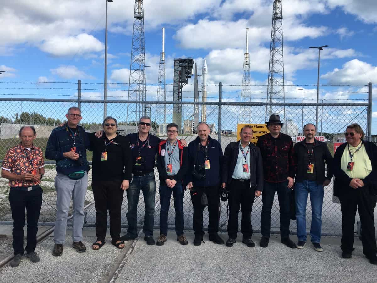
High fliers: Chris Owen (sixth from left) and other principal investigators responsible for the 10 scientific instruments on the Solar Orbiter mission. “This is probably a once-in-a-career kind of picture,” explains Owen, “and was taken a few hours before the mission launch, when we got up close to the launcher.” (Courtesy: Yannis Zouganelis/ESA)
It’s unlikely that Chris Owen, professor of physics at UCL’s Mullard Space Science Laboratory (MSSL), will ever forget where he was on the evening of 9 February 2020. Hardly surprising given that he was high-fiving colleagues in Cape Canaveral, Florida, after witnessing the successful launch of ESA’s €1.4 billion Solar Orbiter mission – a spacecraft that, once it reaches its operational orbit in two years’ time, will use an array of 10 scientific instruments to deliver the most detailed images yet of the Sun and its outer atmosphere as well as unprecedented in situ measurements of the solar wind, the continuous stream of high-speed charged particles emanating from the Sun’s surface.
Owen, for his part, is principal investigator for one of those scientific instruments – the mission’s Solar Wind Analyser (SWA) – and heads up an international science and engineering consortium that will, over the next decade, use the SWA’s sensors to better understand the physics of space weather. Here he talks to Physics World about big-science collaboration and the benefits for UCL’s MSc students of proximity to the staff and projects at MSSL.
What role will the SWA play on Solar Orbiter?
The Sun emits a constant stream of high-speed charged particles into the heliosphere (a vast, bubble-like region that extends from the Sun to the edge of the Solar System). This solar wind influences Earth’s near-space system – sometimes disrupting satellite communications and, on occasion, even damaging or destroying orbiting spacecraft. The SWA will carry out a range of in situ measurements on this particle stream – something akin to “sniffing” the solar wind.
Who built the SWA?
The SWA is a case study in international collaboration. There are three sensors on the instrument: the one we built here at MSSL will study electrons in the solar wind; the sensor for protons and alpha particles was built mostly in France and the Czech Republic; while a US team supported by NASA led the development of the sensor for heavy ions such as iron, carbon and oxygen. All three sensors are controlled by a central electronics box built in Italy, while Airbus UK developed the spacecraft as well as the heatshield technology that will protect it while orbiting close to the Sun.
How do your MSc students benefit from MSSL’s involvement in high-profile missions like Solar Orbiter?
At MSSL, we are the largest university-based space science lab in the UK, covering all core space science and engineering disciplines in one department. At any given time, we’re participating in a range of big science projects that, by definition, have to be multidisciplinary and international in scope. That means our MSc students get to learn from leading space scientists and engineers involved in defining and delivering new space missions. Our MSc is attractive in terms of its subject coverage and scope, but also because of MSSL’s strategic position within the space science ecosystem. We have a lot of connections within the space industry and that can open doors for our researchers and students.
Are there opportunities for MSc students to get involved directly with missions like Solar Orbiter?
Absolutely – that’s the norm rather than exception at MSSL. Last year, for example, one of my MSc students undertook a project to investigate spacecraft charging in the solar wind – and specifically the impact that this behaviour might have on the SWA’s measurements of charged particles. The student in question used simulation tools to build and “test” a virtual Solar Orbiter spacecraft in an effort to understand the underlying physics, with the behaviours predicted by her simulations feeding into the wider ESA research on this issue.
What does the future hold for MSSL and your MSc programme?
These are exciting times for MSSL. We’re working on a number of high-profile future missions, including Plato (to drive new discoveries in exoplanetary science), Euclid (mapping of the dark Universe) and the PanCam scientific cameras for the ExoMars 2020 Rover (scheduled to arrive on Mars in April 2023). All of these missions will translate into incredible learning and research opportunities for our MSc students.