Ulf Leonhardt: transforming optics research

Ulf Leonhardt

How has transformation optics evolved over the past decade since the initial breakthroughs on invisibility cloaking?

The research on invisibility and related effects has become much more diverse – and that’s a good thing. In the long run, I think the applications will not be in optics but in areas like acoustics and other mechanical waves. Essentially, we’re talking about the manipulation of waves with ideas taken from transformation optics and inspired by analogies with space–time geometries. Imagine, for example, you have a bridge and you want to protect or cloak that bridge from potential earthquakes. How do you design the surrounding underground structures to effectively minimize the effect of seismic disturbance? That’s a meaningful question and an active area of endeavour. Acoustics applications are driven by military requirements such as the cloaking of submarines and other naval vessels from sonar. This is not something I’m working on, and even if it was I wouldn’t be able to talk about it!

What are your research priorities at the moment?

Transformation optics is an active area for my group in various respects. One example is the idea of transforming the geometry of space in optical instruments – and specifically planar silicon photonic devices. Fundamentally, this is about shaping light at the chip level and what we can add are some unique design tools and manufacturing tools. This is work that’s heading in an applied direction for the sorting of light on chips in optical switching and optical computing technologies.

Any other areas?

Another theme is the connections between transformation optics and Casimir forces – the forces of the quantum vacuum that are responsible for “stickiness” in nature. Though tiny, Casimir forces become significant at micron and submicron distances. They’re the reason parking tickets attach to a windscreen and, unhelpfully, why parts in nano- and microelectromechanical systems sometimes stick together. There are deep, unresolved problems in this field and it’s worthwhile working on them. It’s subtle, challenging research and it’s off the beaten track. We’ve found surprises already and there will be plenty more that will lead to new and interesting lines of enquiry.

What attracted you to Israel and the Weizmann Institute?

So far, I’ve worked as a researcher in 10 countries, including Germany, where I was born, as well as the UK and Sweden. I came to Israel to settle in 2012 and have invested lots of time and energy in setting new research directions. For now, it looks like a life sentence – the nice sort of life sentence. The Weizmann is an institution for basic research and the most important criterion is that the science is interesting – nothing else. Whether the work leads to some additional funding or practical applications is of a secondary nature. Having said that, there’s a paradox here in that the Weizmann is also the world’s most successful scientific institution in terms of research commercialization. Patent income is a huge part of the financing model.

What is the secret of that success?

It’s because the best applications come from fundamental science. The Weizmann Institute is a graduate university – we have no undergraduates – and a lot of the drive comes from our students. They have an eye for applications, innovation and want to spin off companies – and it helps that the Weizmann has strong ties with industry on many levels. There’s also the commercial environment in Israel, with a significant proportion of GDP – in excess of 30% – coming from hi-tech industries.

What sets the Weizmann Institute apart from other institutions you’ve worked at?

The Weizmann is an institution of international significance with a predominantly Israeli student body and faculty. The quality of our students is a big differentiator. A Master’s thesis here will typically involve 12–18 months of research and the final output is at the level of a UK PhD. For PhD studies, four or five years is completely normal and the research stands in comparison with elite institutions around the world.

How does this help to set students apart?

It’s worth noting that most of our students have been through a period of military service after high school – three years for men, two years for women. As such, they will have worked on science and technology R&D programmes from an early age, often with significant responsibility for budgets and delivery. When they join us at the Weizmann, our students are already mature, independent, responsible and prepared to take ownership – significant attributes when pursuing a postgraduate research path.

Prior to Israel, you spent 12 years at the University of St Andrews. What impact do you think the Brexit impasse is having on UK science?

I know from several senior colleagues in the UK that they are thinking of leaving or have concrete plans to leave because of the uncertainty around Brexit – especially with respect to EU research funding. It makes me very sad because traditionally the UK has been very attractive and welcoming as a destination for European scientists, including myself. The language, the openness of the research institutions, the value placed on individual freedoms: all these factors have made the UK an easy place for foreign scientists to settle and work, while providing a window to the wider world within Europe. It all depends how the political situation works out over the next few months, but right now there’s a serious problem. No doubt about that.

Having spent some time working in China, how do you see the country’s global emergence as a science superpower?

There’s a major debate right now – driven by the trade war with the US – about the global rise of China and what the West must do to respond. China plays a long game, including in science, with government support and co-ordination of that long-term outlook. Europe and the UK – which is still a part of Europe – need to be ready for the challenge before the Chinese Belt and Road Initiative begins to stretch its tentacles into European science, as it has already done in Italy. We live in interesting times, and they will get more interesting by the day. It’s time to wake up.

Do you have any advice for early-career scientists embarking on their chosen research path?

If you want to achieve something difficult in science, you must first believe in it. You cannot be a critic from the outset; if you are, you’re not getting anywhere. At the same time, there’s an important duality or paradox to remember – on the one hand believing something is possible, on the other only trusting the facts and being self-critical at the appropriate time. In my team, we are our own strongest critics. In research, you also need to be patient and to persevere through difficult times. Although, when you find that a given line of enquiry isn’t working you should be honest and true to yourself. Be prepared to write it off and start all over again.

If you want to achieve something difficult in science, you must first believe in it

You have also written a novel. What inspired you to do this?

I have always enjoyed writing stories in foreign languages and so, one rainy winter day in Israel, I began writing a novel. Storytelling is the natural, most human way to communicate and teach anything – even physics. Aspiring novelists are usually advised to write about things they know well, so I wrote a story about the science I do and about travelling the world off the beaten track.

What is it about?

The book is about the science of invisibility and optics more generally. The reader will get an accurate picture of the real science of invisibility and glimpses into different cultures. If a publisher is interested, I would be happy to talk terms.
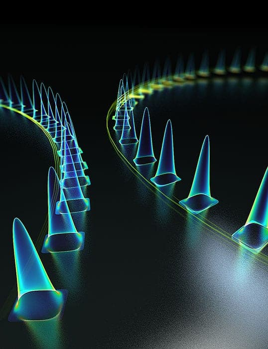

Soliton gas is created in the lab using colliding water waves

A “gas” make from soliton waves has been created for the first time by physicists in France and Italy. The gas was generated inside a shallow wave tank, where individual solitons could ricochet back and forth. The measured properties of the gas match those predicted by computer simulations and the work could improve our understanding of how waves propagate within a variety of real-world systems.

Solitons are wave packets that maintain their shapes and sizes as they propagate over time – even when colliding with each other head-on. First observed in 1834 as water waves on the surface of a canal, solitons can occur in different media – including optical fibres, where solitons take the form of pulses of light.

A soliton resembles a particle because it maintains its shape and size as it propagates. As a result, an ensemble of solitons can be described as a gas of particles. Soliton gases are thought to play important roles in the dynamics of wave propagation in optical fibres, plasmas and water waves in shallow ocean basins.

Testing times

While soliton gases have been modelled in computer simulations, physicists had not been able to test these calculations in the lab. As a result, researchers do not have a good understanding of how wave-damping effects such as friction and viscosity affect soliton gases.

Now, Nicolas Mordant at the University of Grenoble Alpes and colleagues have created an experimental soliton gas in a shallow 34 m-long wave tank – taking advantage of the fact that water waves can behave as solitons at shallow depths. A piston at one end of the tank generates a steady train of waves, which reflect back and forth across the tank. By fine-tuning the amplitudes and distributions of the waves, the researchers were able to maintain a dense, steady-state soliton gas inside the tank.

The highly controllable conditions of the setup mean that Mordant and colleagues can make very precise measurements of the entire spectrum of possible excitations within the tank. Across the spectrum, the researchers observed that although the amplitudes of the solitons inevitably decayed over time due to friction, they maintained their profiles, even after colliding with other solitons travelling in the opposite direction. In addition, the  measurements of the wave heights in space and time remained extremely consistent with those predicted by previous statistical models of soliton gases.

The researchers say that their experiment is ideal for investigating the special case in which time-varying wave dynamics are entirely determined by their initial conditions – the case of “integrable wave equations”. Such analysis would allow for new insights into the dynamics of systems including the propagation of light along optical fibres, the complex interactions characteristic of plasma waves, and patterns of waves in the ocean.

The research is described in Physical Review Letters.

Conservation payments reduce deforestation on land next door

Renzo Guidice with participating community members

Paying indigenous groups to conserve their land could reduce deforestation. But a pilot conservation payment scheme in Peru has had minimal impact, according to a research team from Peru, Germany and Spain. Changing the way that indigenous communities enrol could increase conservation gains significantly, the researchers believe.

Over half Peru’s greenhouse-gas emissions come from destruction of the Amazon rainforest. Around 16% of this deforestation occurs on land belonging to indigenous communities. These communities are some of the poorest population groups in Peru. The forest is an important source of their livelihood, through activities such as traditional “slash and burn” agriculture, logging, renting land to third parties for cash crops such as palm oil and coca, and gold mining.

Back in 2010 the Peruvian Ministry of Environment created a National Forest Conservation Program. Through 2011, 50 indigenous communities enrolled onto the scheme. In return for their ecosystem payments, the communities were expected to implement sustainable forestry projects such as small-scale coffee plantations and sustainable timber harvesting.

Renzo Giudice from the University of Bonn, Germany, and his colleagues used remotely sensed deforestation data gathered between 2001 and 2015 to assess the impact of this pilot conservation programme.

The scheme had low impact, with only minimal levels of avoided deforestation, the results show. The greatest amount of avoided deforestation occurred on lands surrounding the conservation area.

“This ‘spillover’ effect is counterintuitive, but could be related to the implementation of the sustainable forestry projects, leaving people with less time to deforest the surrounding areas,” says Giudice.

But why was the avoided deforestation so low on the lands that were enrolled in the scheme? Giudice and his colleagues believe this is because communities chose which parts of their land to enrol in the scheme, and tended to select areas that were not at high risk of deforestation in the first place.

“We believe that the scheme would have far more impact if communities had to enrol their entire territory, to avoid this self-selection bias,” says Giudice, who published the findings in Environmental Research Letters (ERL). What’s more, the researchers suggest prioritizing enrolment of communities with lands most threatened by deforestation.

Deforestation and forest degradation are the second largest source of greenhouse gas emissions worldwide, so ecosystem payment schemes could play a key role in climate change mitigation. The latest findings suggest that ecosystem payments do have potential, but only if the enrolment conditions are tightened.

Fast-switched dual-energy fluoroscopy tracks tumours during radiotherapy

The ability to track lung tumours during radiotherapy, without the use of markers, could make therapeutic dose delivery more effective and reduce exposure to healthy surrounding tissue. One option, the use of X-ray imaging, has been limited by its inability to adequately visualize a tumour overlapping bone. Researchers from Loyola University Medical Center have now shown that fast-kilovoltage (kV) switching dual-energy fluoroscopy can improve the accuracy of markerless tumour tracking when used with software that removes bone and enhances soft tissue (Med. Phys. 10.1002/mp.13573).

The research team previously evaluated sequential dual-energy imaging using the on-board imager of a linear accelerator (Med. Phys. 10.1118/1.4903892). This research revealed the efficacy of sequential dual-energy fluoroscopy, as well as its limitations, as it produced respiratory and organ motion artefacts. The team hypothesized that by rapidly alternating the X-ray tube potential at a high frame rate, such motion artefacts would be reduced and dual-energy imaging could be performed in real time.

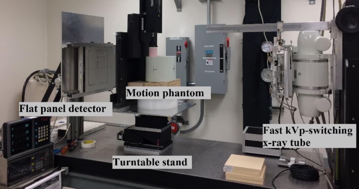
For their latest study, the researchers employed a fast-kV switching fluoroscopy prototype developed at Varian Medical Systems that produced alternating 60 and 120 kVp X-rays. To simulate chest anatomy and tumour respiratory motion in the lung, they used a dynamic thorax motion phantom containing a 3D anthropomorphic spine and ribs and a spherical “tumour” capable of producing complex motion. They imaged five tumour inserts of 5 to 25 mm in diameter. The inserts were programmed to move in the phantom’s inferior–superior direction, perpendicular to the X-ray beam, to mimic respiratory motion.

Fast-kV switching imager prototype

The researchers acquired images at 15 frames/s and created bone-subtracted images using internally developed software. They then calculated tracking success rate and accuracy in regions of the phantom where the target overlapped ribs and spine, to compare the performance of single-energy and dual-energy imaging methods.

The team also varied the CT slice thickness to evaluate and optimize template quality. They determined that a CT slice thickness of 0.75 mm resulted in the lowest tracking error for the smallest 5 mm target.

“The results of our study indicate that there may be a range of optimal slice thicknesses for each tumour size,” the researchers write. For single-energy imaging, the smallest CT slice thickness may be preferable for tumour diameters between 5 and 10 mm, while for larger tumours (15–25 mm) a CT slice thickness of less than 3 mm is desirable. For dual-energy imaging, a slice thickness of less than 3 mm would result in comparable tracking error for all targets below 25 mm in diameter.

“The most significant gains were observed for the smallest simulated tumours, the 5 and 10 mm diameter targets,” explains academic co-principal investigator John Roeske. “In particular, for the 5 mm target, there were cases where the motion was only tracked on a few frames using single-energy imaging. The addition of dual-energy imaging significantly improved the tracking success rate of this small target.”

The authors calculated the tracking accuracy for both single- and dual-energy imaging, using the mean absolute error between the predicted and expected location of the tracked tumour. With the exception of the 5 mm target, dual-energy imaging outperformed single-energy imaging in all simulated motion types. When the 5 mm tumour overlapped the simulated spine of the phantom, dual-energy tracking success rates for static, slow and fast motion were 24%, 38% and 54%, respectively, compared with 0%, 3% and 3% for single-energy tracking. In general, larger improvements were observed for tumours overlapping spine than those overlapping ribs.

The authors also note that higher peak-to-side lobe ratios and improved tracking accuracy of dual-energy over single-energy imaging may offer advantages in the clinical setting, where tumours may have varying densities and less than ideal shapes.

This research was a joint initiative between Loyola University Medical Center and a Varian research laboratory. Roeske tells Physics World that working with industry co-principal investigator Hassan Mostafavi, they are moving their studies from a benchtop system to a linac and have already implemented fast kV switching in Developer Mode of the TrueBeam️ radiotherapy system. They are also repeating a number of studies to validate their findings using the benchtop system. After they complete these studies, the goal will be to evaluate their approach, with IRB (institutional review board) approval, on a small cohort of patients.

When asked to speculate on when this markerless tumour tracking technology could be used in clinical settings, Roeske says that lead author Maksat Haytmyradov will present the initial characterization of fast-kV switching at this year’s ASTRO annual meeting.

The promise of silicon photonics

The world’s appetite for data is growing exponentially, driven by applications ranging from social networks and streaming media to genomics-driven medicine and the proliferation of connected devices within the “Internet of Things”. The growth in mobile computing is especially stark. According to the United Nations’ telecommunications agency, by 2013 the number of mobile phone subscriptions was already approaching the number of humans on Earth. Landline telephones, in contrast, have never reached more than 25% of the global population.

The bountiful opportunities provided by these technologies and services – and by whatever comes after them – ensure that people will continue to find new ways for data to connect, entertain, inform and help us. But this increased data use comes at a cost. In 2009 Google revealed that a single Internet search consumes about 1 kJ of energy. By 2016 industry experts estimated that the world’s data centres – massive monoliths of servers and switches – were consuming almost 40% more electricity than the entire UK. The figure has likely grown since then, as increases in data volumes have so far outstripped improvements in efficiency.

Another challenge for our data-intensive world is that even at the level of consumer devices, data rates are starting to exceed the capability of conventional interconnect technologies. For example, the extraordinary pixel density and high frame rates of the latest high-definition televisions are rendering conventional copper HDMI cables increasingly ineffective. Even over the relatively short distances found in home entertainment systems, the degree of signal degradation in such cables is significant.

The central problem here is that conventional, electronic data systems require wires to be charged and discharged in order to send a bit of data from point A to point B. Even in the microscopic wires found inside CPU and RAM chips, this charge-discharge cycle takes both energy and time. As David Miller, an applied physicist and electrical engineer at Stanford University in the US, has pointed out, most of the energy used in information processing goes towards communications, not logic. Even at the gate level, the main driver of energy dissipation is the capacitance of the wires being charged and discharged, which amounts to about 200 attofarads (10–18 F) per micron of wire. At the data-centre level, the largest server farms may consume an entire power plant’s worth of electricity, so the efficiency of server-to-server interconnects poses serious sustainability issues.

Many of these issues would be substantially mitigated if cables and switches were configured to communicate using photons rather than electrons. The promise of photonics in computing and communications actually extends far beyond this, encompassing new possibilities for logic and processing as well as some approaches to quantum computing. Those applications lie in the near- to mid-term future, but photonic interconnects are available today, with advantages including scalability, capacity, parallelism, longer link-lengths and speed. Even consumer applications benefit. Optical HDMI cables can now support high frame rates for displays 4000 or 8000 pixels in width (and beyond) over commercially useful cable lengths, and optical USB and Thunderbolt implementations are emerging for data rates of 40 Gbps and upward.

Manufacturing these photonic devices isn’t easy, however. Sure, the process begins with the same silicon wafers that have been ubiquitous in microelectronics for decades, and it uses many of the manufacturing tools found in standard semiconductor fabs to print optical components and circuitry onto wafers alongside (or instead of) microelectronic elements. However, photons fundamentally do not obey the same physics as electrons. Guiding a photon from one element to another inside a packaged “chip” is not as simple as soldering the two together. For one thing, alignment tolerances are much more exacting. Whereas connecting a wire to a contact-pad on a chip involves aligning the components to within a few tens of micrometres of the correct position, connecting an optical fibre to a photonic chip can require three orders of magnitude more precision. Fortunately, thanks to ingenious device engineering and some groundbreaking micro-robotic industrial automation technology, we are well on our way to overcoming these challenges, bringing high-throughput photonic interconnects into the mainstream.

Precedents for progress

The challenges involved in manufacturing systems that use photons to transmit information are not new. In fact, they date at least as far back as the late 1990s, when photonics technology was first deployed on a grand scale to replace satellite links in long-distance telecommunications. At the time, the task of sending light from then-novel laser diodes down a single-mode optical fibre required the positions of both components to be laboriously adjusted before the laser’s light was efficiently coupled into the fibre. An analogue technology called a gradient search was a partial solution, enabling the positioning system to quickly reach an optimum transmission value (at least for fibres with a smooth modal profile). However, the positioning systems themselves had significant limitations. They were often fragile, with limited travel ranges and a tendency to drift out of alignment – not good qualities for systems being deployed in industrial environments. The problem was ultimately solved by developing a digital version of the gradient search and deploying it on industrial-class motion hardware that had already proven its worth in semiconductor manufacturing. The combination provided a path forward for manufacturing robust hardware for optical fibre interconnections.

Today’s photonic data devices are significantly more sophisticated and complex. Thousands of photonic integrated circuits (ICs) can be minted on a single wafer, offering the tantalizing potential for processing multiple channels of light at once, increasing capacity and speed. Photonics ICs today routinely integrate both multi-channel and multi-wavelength structures, with inputs and outputs arranged in arrays that enable each device to process and carry multiple channels of information.

In some respects, though, the challenge of making these circuits “talk” to each other is the same as it was for telecoms fibres. All of the chip-level photonic inputs and outputs need to be coupled to other elements, including optical fibres, fibre arrays, waveguide-based structures, laser diodes and bulk elements such as lenses and gratings, as well as other chips. Many of these couplings require meticulous alignment not only in the sensitive transverse plane (by convention referred to as the “XY” plane) but in other degrees of freedom. Importantly, an array of photonics devices must be precisely oriented not only in the XY plane but also in the theta-Z direction, and often in other degrees of freedom (DOFs), too.

Another complication is that the necessary alignment can only be performed actively – by measuring the actual coupling of light into the fibre. This is because the machine-vision approaches commonly deployed to determine device positions during assembly cannot resolve spatial tolerances of tens of nanometres, and passive-alignment approaches (such as precision V-grooves, in which fibres are glued in place) typically require impractical device replication tolerances.

In principle, the 1990s-era digital gradient search would still work for aligning the optical components in silicon photonics. In practice, however, the number of array elements involved, combined with the need for multi-DOF optimization, means that the process of finding a globally optimal alignment is not straightforward. Moving a certain component in the theta-Z axis, for instance, will inevitably cause it to de-align in the XY plane due to the mechanical rotation axis not being precisely coincident with the optical axis.

This problem has often been solved using a looping approach: you align the component in XY; make a small theta-Z improvement; go back and re-align in XY; and then iterate until the result is satisfactory. Looping is also deployed to optimize devices (such as the short, multimode waveguide structures common in silicon photonics) that exhibit interactions between channels and between inputs and outputs. In this case, you start by optimizing the input, then optimize the output – except now the input is no longer optimized, so you loop until you achieve a consensus optimum. Once the optimization process is complete, digital gradient search technology can track the elements’ alignments, ensuring that they stay optimized in the face of drift from thermal changes and the stresses involved in curing glued elements.

Killing off the loops

There’s just one catch: looping is far too slow to be practical for testing and later assembling the thousands of devices from each wafer. To understand why, consider the early stages of wafer manufacturing. As in conventional microelectronics manufacturing, the cost of minting a silicon photonics wafer constitutes only a small part of the finished price of a packaged chip. Since wafer yields are by no means 100%, it makes good economic sense to discard faulty devices before they reach the packaging phase, where costs are considerably higher.

In microelectronics manufacturing, this quality-control process is carried out using specialized tools called wafer probers that subject each chip to contact from precise, needle-like electrodes that stimulate it and observe its response, often via racks of sophisticated instruments. To carry out the same tests on a photonic chip, however, it is not enough just to make electrical contact. Light must also be coupled into and out of the chip’s embedded photonic circuitry, and the chip’s performance measured by optical means. Array elements pose special challenges, since the devices must be rotated into precisely matching orientations as well as translated into tight transverse alignment. Traditionally, optimizations of this sort needed to be performed in a stepwise fashion, with angular adjustments interleaved with transverse re-alignments to compensate for any mismatch between the optical and rotational axes. This could take several minutes – an unacceptable (and uneconomical) length of time, given that each wafer can contain thousands of silicon-photonics chips.

Recently, a solution has emerged in the form of a new approach to digital gradient search that enables industrial positioners to perform gradient searches across multiple channels, inputs and DOFs at the same time. Instead of iteratively making small theta-Z motions interleaved with XY corrections over a span of perhaps minutes, this technology can perform the XY and theta-Z alignments simultaneously, using two gradient-search processes in parallel. This parallel digital gradient search (PDGS) approach can be scaled up to the full six degrees-of-freedom for each device, and multiple positioners can work cooperatively on multiple inputs and outputs of a device even if there are interactions between the inputs, outputs and channels.

Thanks to PDGS, the minutes-long, serial process of looping (for example) the XY and theta-Z alignments of an array device reduces to only a second or so – a time savings of 99%. The parallelism of the technology also means that the overall process time is almost independent of the number of adjustments performed. This is significant because in manufacturing (as in so many things), time is money. It is no surprise that manufacturers and users of wafer probers were the first to incorporate micro-positioning robots that use PDGS, with the first implementations in 2016. The microrobots have also been implemented in other areas of manufacturers’ assembly processes, such as aligning chips and other components together in their packages. Some manufacturers have even instituted specialized test tools for re-validating the health of the chips at intermediate steps in the packaging process. This parallel process has been implemented within the firmware of the industrial-class, six-DOF hexapod microrobots and other precision mechanisms used in manufacturing silicon photonic devices, transforming the unfavourable economics of the silicon photonics industry.

Parallelism beyond silicon

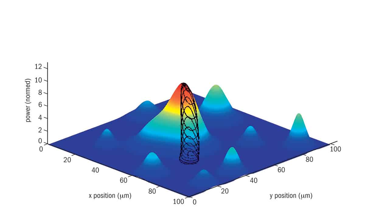
When assembling and testing silicon photonics devices, the parameter being optimized is almost always optical power. However, many other relevant metrics also exhibit a similar sort of roughly hill-shaped optimization trend, and PDGS does not require its inputs to have a purely Gaussian profile (which is a good thing, as silicon photonics devices rarely produce light beams with clean Gaussian profiles). Secondary maxima or “foothills” around the main peak are no problem, as the main mode can usually be selected by performing an area scan. A classical version of this would be a raster scan that sweeps over a defined area, but the microrobots implement a considerably faster approach in the form of a vibrationless sinusoidal or spiral area scan built into the firmware at the command level (see image on p31). This allows the main coupling peak to be identified, ensuring that the gradient search locks onto and tracks the main mode.

This opens the potential for applications of PDGS unrelated to silicon photonics. In laser manufacturing, for example, bulk optics are aligned to a mutual optimum based on various parameters of the output beam. This can be a time-consuming process, so automating it promises significant rewards in terms of yield and production throughput. Cameras are another example. Billions are manufactured every year, largely driven by the world’s demand for smartphones, by the smartphone industry’s steady progress in camera quality and by novel applications such as facial mapping. Each generation of phones integrates more cameras per handset, to the extent that smartphone demand could plummet 50% (something that is not going to happen, I hasten to add) and yet smartphone manufacturers would still require more cameras in 2019 than they did in 2015. Camera adoption in cars and trucks is also skyrocketing, propelled by rapid adoption of safety technologies and autonomous driving capabilities.

With more optical devices of greater sophistication being manufactured each year, the applications of PDGS will continue to expand. By giving nanoscale eyes to microrobots, this technology makes it possible to optimize the position of multiple optical elements in both silicon photonics and other areas of manufacturing – thereby keeping precision positioning up to speed with new chapters being written in computing, imaging and many other areas of photonics technology.

  • Enjoy the rest of the 2019 Physics World Focus on Optics & Photonics in our digital magazine or via the Physics World app for any iOS or Android smartphone or tablet.

Magnetic topological insulator goes clean

Researchers have discovered the first ever intrinsic magnetic topological insulator – a stoichiometric compound that boasts both inherent magnetic order and topological insulator characteristics. The material, MnBi2Te4, which is made by growing quintuple Bi2Telayers and a MnTe bilayer, could be the ideal platform in which to study exotic quantum phenomena such as the quantum anomalous Hall effect (QAHE) and quantum phases like axion insulators at higher temperatures.

Topological insulators are electrical insulators in the bulk but can conduct electricity extremely well on their surface via special, topologically protected, electronic states – hence their name. The materials are predicted to exhibit various exotic quantum effects, but many of these effects can only occur if magnetism is introduced. One example is the QAHE, which is a quantum Hall effect that can occur without an applied magnetic field.

In topological insulators exhibiting the QAHE, electrons can only travel in one direction and do not backscatter. This means that they can carry electrical current with near-zero dissipation of energy and so could be used to make energy-efficient electronic devices in the future. Topological insulators normally need to be doped with magnetic impurities to introduce magnetism into them, but this also introduces strong disorder.

“Such ‘dirty’ materials are a nightmare for researchers studying the quantum effects therein,” explains Ke He of Tsinghua University in Beijing.  “Another consequence of the strong disorder is that the temperature at which the QAHE appears is extremely low – at about 0.1 K.”

Intrinsically magnetic topological insulator is stochiometric

An intrinsically magnetic topological insulator solves this problem since it is stochiometric and has orderly arranged magnetic atoms, he adds. “We have now found such a material – a topological insulator with intercalated magnetic layers.”

The researchers used molecular beam epitaxy to grow MnBi2Te4 films. This technique allows them to accurately control film thickness – on the order of one atomic layer, in principle – as well as minimize contamination from the environment.

“For MnBi2Te4, our procedure is a little special,” explains He. “We repeatedly deposit one unit of Bi2Te(which includes five atomic layers) and one unit of MnTe (which includes two atomic layers). This leads to MnBi2Te4 spontaneously forming – something that we confirmed in high-resolution transmission electron microscopy images.”

Dirac-cone-shaped surface

The films also have Dirac-cone-shaped surface states, which is characteristic of a 3D topological insulator, he adds. Dirac cones are features in the electronic band structure of a material where the conduction and valence bands meet in a single point. Electrons in these cones behave as though they are relativistic particles with no rest mass, travelling through the material at extremely high speeds – a property that could be exploited to make ultrafast transistors, for example.

The films are magnetic too, which means they can exhibit the QAHE.

“Our theory colleagues have also found several different topological phases that could reside in the material with different thicknesses and magnetic structures,” says He. “The material thus provides us with a perfect platform to study various topological states of matter.”

Quantum effects at higher temperatures

The intrinsically magnetic topologically insulating films are more ordered than their magnetically doped counterparts and could thus exbibit quantum effects at higher temperatures, he adds. “Indeed, recently two groups have observed the QAHE at 1.5 K in exfoliated flake samples of the material, which compares well with the best magnetically doped topological insulator samples. I believe that we could reach higher temperatures by further optimizing the quality of the samples.”

Such a system could be used to explore chiral Majorana modes by depositing a superconductor on the topological insulator, he explains. Majorana modes have zero charge and are their own antiparticles and unlike conventional fermions such as electrons (which obey Fermi–Dirac statistics), Majorana zero modes obey “non-Abelian” statistics. This means that they could be used in quantum computing applications since the quantum information encoded in the particles would be highly resistant to decoherence – a property that is required in any practical quantum computer.

“Although researchers have tried to observe these modes in magnetically doped topological insulator-superconductor junctions, the strong disorder in the materials made interpreting the data difficult,” says He. “Our intrinsically magnetic topological insulator may be better here.”

Topological magnetoelectric effect

The MnBi2Te4 may also become an axion insulator – the solid-state version of the axion, which is a very interesting elementary particle in high-energy physics, he adds. An axion insulator is expected to show the topological magnetoelectric effect. This is different to the usual magnetoelectric effect in that the coupled electric field and magnetic field are collinear (rather than being perpendicular to each other) and are related by a quantized coefficient. This special effect may have some important applications as well as having implications for metrology.

The researchers, reporting their work in Chin. Phys. Lett. 10.1088/0256-307X/36/7/076801, say they will now be looking into other intrinsically magnetic topological insulators and hope to find the effect in thicker magnetic layers. “Such materials should be more stable in their ferromagnetism thanks to much weaker spin fluctuations than the present single-atomic-layer layer samples and could thus show the QAHE at much higher temperatures than described in our current work,” says He. “I imagine that this temperature could exceed liquid nitrogen temperatures (77 K),” he tells Physics World.

AI predicts coma outcome from EEG trace

Marleen Tjepkema and Michel van Putten

When patients suffer cardiac arrest, more than half of those who remain comatose never regain consciousness. Early and accurate prediction of neurological outcome is hence key when deciding whether to treat or not. Researchers from the Netherlands have trained an algorithm to read electroencephalograms (EEGs) and predict outcomes. They found that the algorithm’s results matched those of trained specialists (Crit. Care Med. 10.1097/CCM.0000000000003854).

Conventional methods to predict outcomes include applying an electrical signal to the wrist of a patient in a coma and checking for correlated brain activity. Failure to do so indicates very low odds of seeing the patient awakening one day. Another method consists of trained specialists analysing EEG traces – recordings of the brain electrical activity – as specific features can give hints of the outcome. For example, a flat EEG is associated with a poor outcome while a continuous EEG is often an indicator of a more favourable result.

The importance of the first 12 to 24 hours

Visual analysis of EEGs does not, however, capture their integral richness and is prone to intra- and inter-observer variability. EEGs also require highly trained analysts, who might not always be available to provide a prognosis within the paramount 12 to 24 hr window.

To remedy this, Marleen Tjepkema from the University of Twente decided to train deep convolutional neural networks (CNNs) to analyse the EEG and provide an outcome prediction. The CNN uses the ECG trace as an input that goes through a set of connected filters and mathematical functions that can extract specific features, in a similar way to neurons in the brain.

In the study, Tjepkema and her team examined 10 s EEG readings from 18 different channels, collected 12 and 24 hr after a cardiac arrest. Five nearby hospitals were involved: two centres provided the training, cross-validation and internal validation datasets, the other three supplied the data that would serve for external validation. In total, 661 patients were used to train the algorithm and 234 patients provided the validation dataset. All patients, apart from 31 lost to follow-up, were checked six months after the samples were recorded, to determine their cerebral performance category (CPC) score that defines their outcome as good or poor.

Matching trained specialists

In the training datasets, sensitivities for the prediction of poor outcomes were 42% and 57%, at 12 and 24 hr after cardiac arrest, respectively. Another important metric is the false positive rate (FPR), the prediction of one outcome when the opposite ends up happening. In both cases, the FPR for poor outcomes was 0%. Positive outcomes could be predicted with sensitivities of 48% and 33%, at 12 and 24 hr after cardiac arrest, respectively, both with an FPR of 5%.

In the validation dataset, 12 hr after cardiac arrest, the algorithm predicted poor outcomes with a 58% sensitivity and a 0% FPR, while it reliably predicted good outcomes with a 48% sensitivity and an FPR of 5%. Interestingly, predictions were less accurate 24 hr after cardiac arrest.

Using the complete dataset, six trained specialists performed visual assessment based on features associated with specific outcomes. Synchronous burst suppression on all channels was associated with a poor outcome, with a sensitivity of 37% at 12 hr and 25% at 24 hr (FPR of 0% in both cases). Conversely, a continuous EEG pattern correlated to positive outcome (sensitivity of 50% at a 9% FPR after 12 hr; sensitivity of 68% at a 20% FPR after 24 hr).

With these promising results, the researchers have shown that machine learning algorithms provide diagnostic information with similar, if not better, accuracy to human experts. Their focus is now shifting to understanding the patterns that the CNNs associate with specific outcomes, in the hope that this will provide new insights into the brain activity of comatose patients.

Reduced adhesion between tissues could create microscopic tumours

Altering the adhesion at the interface between tissues with different steady-state pressures allows the stable coexistence of the tissues – according to simulations done by physicists in Germany. Their study produced a variety of coexisting structures including spheroids akin to microscopic tumours. This has led the researchers to suggest that a reduction in adhesion could be involved in the formation of the very small, symptom-free occult tumours, which occur so abundantly in tissues.

The inherent steady-state (homeostatic) pressure of a tissue is caused by the dynamics of cell growth, division and cell death. This pressure is known to be an important factor in how different tissues compete for growth space. Cell culture and computer modelling has shown that the tissue with higher homeostatic pressure overcomes the lower-pressure tissue and eventually annihilates it. But Jens Elgeti from the Institute of Complex Systems at the Research Centre in Jülich, Germany, felt this conflicted with basic tumour biology.

“Tumours are very heterogeneous, with lots of different cells within the same tumour, so if one cell always out-competes the others, this tumour heterogeneity should not happen!” explained Elgeti. To gain a better understanding of this dilemma, Elgeti and colleagues have done a computational study of how tissue interactions affect this competition process.

How to coexist

The team took a physicist’s minimalistic approach, with the biology and biochemistry considered constant. Their model integrated mechanical factors such as the rate of cell removal by apoptosis (the normal death of cells) and external fluctuations driven by the dynamic extracellular matrix. This quantitative model has been previously shown to reasonably agree with experimental growth of cell spheroids.

The two tissues, dubbed A and B, are considered in the model and were given different homeostatic pressures. As expected, the tissue with the higher pressure annihilated the lower pressure tissue. Having established their model, Elgeti’s team started to change individual properties at the interface between the tissues. One property that they investigated is cross-adhesion, which is the sticking of cells from tissue A to tissue B, and vice versa.

Cells without cross-adhesion didn’t die, instead they developed a fascinating steady-state coexistence

Jens Elgeti

“There was a prediction in the literature, that if you have no adhesion it generates surface tension and kills any microscopic lesions, but it just didn’t work, the cells without cross-adhesion didn’t die,” explains Elgeti. “Instead they developed a fascinating steady-state coexistence,” he adds.

The simulations suggest that several stable 3D structures can coexist within a host tissue. These include spherical and cylindrical inclusions as well as layered and bi-continuous structures.

Growing together

The team then sought to understand the physical mechanism by which reduced adhesion at the tissue’s interface caused coexistence. After many attempts at cracking this question, they settled on using the slab-like coexisting geometry as the most simplistic system on which to develop an analytic model. This geometry comprises blocks of A and B tissues that abut each other at a planar interface.

They found that the reduced cross-adhesion enabled tissues to grow at the interface, and that this increased growth rate stabilized the net-apoptotic bulk. The team quantitatively described the mechanics involved, and their equations support the simulations.

Roger Bonnecaze from The University of Texas at Austin, who specializes in modelling complex materials such as tissue, commented, “The [research] provides a very provocative perspective on how two different cell types can coexist and this should encourage experimentalists to try and verify these predictions.”

Insights into tumour biology

Elgeti’s team suggest that the link between cross-adhesion and tissue coexistence could contribute to the stable coexistence of microscopic lesions, which are thought to occur in abundance in every human body. But they are also excited about the role their mechanism might play in cancer evolution – the series of steps that alters a healthy tissue into a malignant tumour. So the team have started to investigate what happens when gradual changes are made to adhesion strength.

“Here we tried the extreme [no cross-adhesion], but as cross-adhesion approaches the bulk-adhesion strength, coexistence disappears and is replaced by random mixtures of both cell types. The very existence of heterogeneous states opens novel routes for understanding tumour evolution,” said Elgeti.

Bonnecaze is interested in the perspectives raised by the research but is uncertain as to whether mechanical perspectives will impact cancer treatment, which fundamentally attacks the biochemical activities that drive these processes. However, he is intrigued by how these mechanisms could aid the integration of tissues within artificially synthesized organs.

The research is described in the New Journal of Physics.

X-ray diffraction reveals switching mechanism in phase-change materials

Phase-change materials can be reversibly switched between their glassy and crystalline states by applying a voltage that heats up the material or by directly heating them up with a laser. Being able to switch between these two “0” and “1” states – a crystalline state with high electrical conductivity and a meta-stable amorphous state with low electrical conductivity – makes these materials promising for new types of non-volatile memory that could help meet the world’s ever-increasing demand for digital information, the volume of which is doubling every two years.

Researchers led by Klaus Sokolowski-Tinten of the University of Duisburg-Essen and Peter Zalden from European XFEL in Germany have now succeeded in observing the processes that occur during switching – something that has never been done before because of the short time-scale involved. The work will be important for designing improved PCMs in the future, they say.

The researchers used hard femtosecond-long X-ray pulses from an X-ray Free Electron laser (the Linear Coherent Light Source – LCLS – at SLAC) to resolve the atomic structure of two PCMs, Ag4In3Sb67Te26 and Ge15Sb85, during the entire switching cycle. Both these materials are used as PCMs in optical (Ag4In3Sb67Te26) and electronic (Ge15Sb85) memory devices.

Two liquid states

To their surprise, they found that two liquid states of the materials are involved in the process – one that has more rigid chemical bonds, and which helps stabilize the glassy “off” state at ambient conditions, and one that is rather metallic and can therefore crystallize very quickly to produce the “on” state.

“These results provide a microscopic understanding of how PCMs work,” explains Zalden, who is lead-author of the study, “and why some materials – like Ag4In3Sb67Te26 and Ge15Sb85 – are PCMs while others (such as Ge15Te85) are not.”

Diffract-before-destroy

The researchers used the LCLS because at the time of the experiment it was the only X-ray source able to resolve the phase change process with a single X-ray pulse. “We can only use one pulse because the PCMs degrade when exposed to high intensity X-rays,” says Sokolowski-Tinten. “XFELs thus offer us the possibility of probing the atomic structure of these materials before the X-rays destroy them.

“We made use of a pump-probe scheme and combined this X-ray source with a laser-melt-quench technique in which we heat the PCM and transform it into the liquid state using an optical laser pulse (just like on optical re-writeable discs, where PCMs are also employed).”

The liquid rapidly quenches into a super-cooled state (that is, one whose temperature is lower than the melting temperature of the material). From here, the material then either crystallizes or forms a glass.

Reconstructing the entire switching cycle

By measuring the atomic structure of the material at various times after optically exciting it, the researchers say they can reconstruct the entire switching cycle. Each pump-probe event has to be performed on a fresh part of the material, however, because of the destructive impact of the X-ray pulse, explains Sokolowski-Tinten.

According to the team, the transition in PCMs comes mainly from the onset of Peierls distortions. This mechanism is a fundamental process that lowers the energy of a material by breaking its symmetry.

“In our case, the octahedral, six-fold coordinated environment of the high-temperature liquid in Ag4In3Sb67Te26 and Ge15Sb85 is distorted in the low-temperature liquid by displacing an atom along a diagonal of this configuration – if the liquid is quenched fast enough to sufficiently low temperatures, as in our experiments,” says Zalden. “This quenching shortens three chemical bonds and elongates the three opposite ones. As confirmed by the simulation results of our collaborators from RWTH Aachen, the bond shortening localizes the valence electrons, turning the materials from being metallic in the high-temperature liquid to covalent in the low-temperature liquid.”

Just as metallic materials are known to be very ductile, the atoms in the high-temperature state are very mobile, he adds. This allows the atoms in the high-temperature state to arrange themselves very quickly on a periodic lattice (and crystallize). The covalent bonds of the low-temperature liquid, on the other hand, are more like those of window glass and help stabilize the glassy state of these materials.

A new design parameter

“The results point to a new design parameter for when it comes to making future PCMs – the ratio of liquid-liquid transition temperature over the melting temperature,” says Zalden. “In a ‘good’ PCM, this value needs to be low and has to induce a strong Peierls distortion. Here, crystallization can take place at the highest rates over a wide range of temperatures and the glassy state is stable over the long-term at ambient conditions.

“More generally, the work and our time-domain approach, can also help us to understand how liquids of other classes of materials behave when they are rapidly cooled to temperatures well below the melting point,” he adds, “and why some liquids are more likely to form a glass than others.”

The researchers, reporting their work in Science 10.1126/science.aaw1773, say they now plan to perform similar measurements on other classes of materials. “We believe that a related structural phase transition mechanism could be occurring during the rapid cooling of materials like silicon,” says Sokolowski-Tinten. “In these materials, we observe different atomic structures between the glass and the liquid, but it is not possible to observe the transition between the two because of the rapid onset of crystallization upon quenching.

“Such studies should allow for a more efficient design of new technical glasses for specific applications, allowing these materials to be used wherever crystalline materials are employed today,” he tells Physics World.

The study, coordinated by the University of Duisburg–Essen and European XFEL and carried out at the Linac Coherent Light Source of SLAC National Accelerator Laboratory in the US, was part of an international collaboration that includes scientists from Forschungszentrum Jülich, Institut Laue-Langevin, Lawrence Livermore National Laboratory, Lund University, Paul Scherrer Institute, SLAC National Accelerator Laboratory, Stanford University, The Spanish National Research Council (CSIC), University of Aachen and the University of Potsdam.

Farmers adapting for ‘weather variability’ not climate change

Be it drought, severe storms, an early spring, wildfires or flooding, farmers are on the front line when it comes to climate change. You’d think they and the people who advise them might be the first to worry about global warming and look for ways to mitigate losses from climate change. But it isn’t this straightforward.

People working in agriculture often don’t link weather extremes and crop losses to climate change, according to recent studies. But the findings also show that farm advisers acknowledge weather variability and are open to adapting farming practices, particularly if they can see the economic and environmental benefits.

“Weather variability perceptions, not climate-change belief, have the strongest correlation to predicting farm advisors’ perceptions of future farmer needs,” says Meredith Niles from the University of Vermont, US. “In short, language matters and how we talk about these issues is important to consider.”

Nile and colleagues analysed historical crop loss data across the US and compared it with surveys of farm advisors carried out by the University of Vermont and the US Department of Agriculture. The team was keen to see if there was a relationship between climate-related crop losses and perceptions of climate change.

Advisors who worked directly with farms on disaster and crop loss issues were often less likely to believe in anthropogenic climate change, they found. However, they were more likely to link crop losses with perceived greater variability in the weather. And it was this perceived weather variability, not climate change, that tended to drive the desire to implement adaptations and plan for the future.

Writing in Environmental Research Letters (ERL), Niles and colleagues suggest that farmers and their advisors are more likely to be influenced by weather variability because it is more observable and less politicized than climate change, and experienced at a personal level.

Another study that surveyed beef and grain producers in Alberta, Canada, showed that farmers were rapidly adopting agricultural practices that had climate mitigation benefits, but not because they believed in anthropogenic climate change. Instead the questions revealed that farmers embraced adaptations because of the expected economic benefits, the anticipated improvements in soil quality and improvements in biodiversity.

“Agreement with the science of climate change is not a necessary pre-requisite for supporting mitigation strategies,” write Debra Davidson of the University of Alberta and colleagues in ERL.

The take-home message from both studies seems to be that farmers might not believe in anthropogenic climate change but are astute observers of the weather and pragmatic about the need to adapt and look to the future.

Copyright © 2026 by IOP Publishing Ltd and individual contributors