Adding retinoic acid from day 4 to day 7 induces stem-cell-derived cardiomyocytes to form tissue resembling atrial heart muscle. (Courtesy: Stem Cell Reports 10.1016/j.stemcr.2018.10.008/CC BY 4.0)
More than 33 million people worldwide suffer from atrial fibrillation, an irregular and often rapid heart rate that can increase risk of stroke, heart failure and other cardiac complications. Studying atrial biology may offer insight into treatment development.
One obstacle to the development of anti-arrhythmic drugs is the difficulty of isolating and maintaining human atrial cardiomyocytes (cardiac muscle cells). Atrial cardiomyocytes, together with the ventricular cardiomyocytes, form the muscular walls of the heart — the myocardium — and make an important contribution to the refilling of ventricles with blood, which enhances the subsequent ejection of blood from the heart. Because animal models do not accurately represent human cardiac physiology, cardiomyocytes derived from human induced pluripotent stem cells (hiPSC) may represent a solution for evaluating potential drugs.
With this in mind, scientists from Germany and the UK have evaluated the suitability of hiPSC-derived atrial-like cardiomyocytes (hiPSC-CMs) as a 3D model of the human atrium. A 3D model offers a physiological cell environment and allows the study of heart function parameters. The findings of this study offer a new platform for the investigation of heart function parameters and pharmacological responses (Stem Cell Reports 10.1016/j.stemcr.2018.10.008).
Model creation
To generate a 3D model of the human atrial heart muscle, the authors induced an atrial phenotype in hiPSC-CMs using previously established retinoic acid (RA) protocols. RA is a vitamin A metabolite involved in the switch between cell proliferation and differentiation.
The RA treatment caused the hiPSC-CMs to achieve properties characteristic of the atrial heart muscle: a decrease in cell size, together with an increase in gene expression and protein level of atrial-specific markers (especially MLC2A, a protein that modulates cardiac development and contractility) and ion channels (potassium channels). These markers indicate that RA promotes atrial-like cardiomyocytes to develop instead of ventricular-like cardiomyocytes. Moreover, the authors noticed that the hiPSC-CMs beat and contracted faster upon RA treatment.
Electrophysiological characteristics
The team used electrophysiological characteristics, such as the action potential duration and the repolarization fraction, to distinguish between atrial and ventricular-type functionalities. RA treatment resulted in a reduced action potential duration and an increased repolarization fraction in hiPSC-CMs, which correspond to an atrial-like electrophysiological phenotype.
In the human heart, two potassium currents are predominantly expressed: the acetylcholine-activated potassium current and the ultrarapidly activating delayed rectifier potassium current (IKur). When the researchers added carbachol, a drug that activates and binds acetylcholine receptors, they observed a shortening of action potential duration in the RA-engineered heart tissue. In addition, when they applied 4-aminopyridine (the inhibitor for IKur), the expected changes in action potential morphology were observed in the RA-engineered heart tissue. These findings suggest that following RA treatment, a more atrial-like electrophysiological phenotype was obtained for the engineered heart tissue.
This study indicates that RA-treated hiPSC-CMs develop an atrial phenotype and form spontaneously beating engineered heart tissue. This tissue shows characteristic atrial heart muscle features, in terms of gene expression, contraction kinetics, action potential features, and pharmacological responses to potassium current blockers and activators. The 3D engineered atrial heart may serve as a useful model in preclinical drug development.
A neutral plasma has been cooled to the record-breaking low temperature of 50 mK by Thomas Langin, Grant Gorman and Thomas Killian at Rice University in the US. In the future, ultracold plasmas could provide important insights into the interiors of giant planets and white-dwarf stars – and could even lead to the creation of exotic states of matter such as a solid plasma.
A neutral plasma can be thought of as a cloud of ionized atoms along with the free electrons the atoms have given up. Plasmas are normally hot because it takes a great deal of energy to keep atoms ionized. However, it is also possible to make a cold plasma in which the ions move slowly (and are therefore cold) while the electrons move much more quickly.
Starting about 20 years ago, Killian has been developing techniques for creating ever-colder plasmas from laser-cooled atomic gases. One important goal of his research has been achieved in this latest work – the creation of a strongly-coupled plasma in which electrostatic interactions between ions define the physical properties of the system.
Millions of strontium atoms
Killian and colleagues begin with a gas of about 500 million strontium atoms that is chilled to 1 mK using standard laser-cooling techniques and held in a magnetic trap. The trap is then switched off and the gas allowed to expand for 6 ms before about 10% of the atoms are ionized by a deep-ultraviolet laser pulse. The liberated electrons, which themselves have a temperature of about 15 K, remain in the vicinity of the ions because of electrostatic attraction. As a result, the plasma is electrically neutral to within a few percent. Infrared lasers are then used to cool the ions to temperatures as low as 50 mK.
An important thermodynamic parameter describing plasmas is the ratio of the electrostatic repulsion between the ions to the kinetic energy of the ions. In these ultracold plasmas, Killian explains, the interactions between ions are more important for defining the properties of the plasma than are the motions of the ions – the hallmark of a “strongly coupled plasma”
Distant worlds
It turns out that this ratio is roughly the same for the high-temperature, high-pressure plasmas that are currently being used in the laser-driven ignition of nuclear fusion. A similar ratio is also found within giant planets such as Jupiter and white-dwarf stars where the crushing force of gravity pushes hydrogen atoms so close together that they form a hot, dense plasma. As a result, ultracold plasmas could be used as simulators that could boost the development of fusion energy sources and improve our understanding of stars and planets.
“We can’t study strongly coupled plasmas in places where they naturally occur,” Killian says. “Laser cooling neutral plasmas allows us to make strongly coupled plasmas in a lab, so that we can study their properties.”
“Strongly coupled ions can’t be near one another, so they try to find an arrangement where the repulsion from all of their neighbours is balanced,” adds Killian. “This can lead to strange phenomena like liquid or even solid plasmas, which are far outside our normal experience.”
GE Healthcare and Vanderbilt University Medical Center (VUMC) have announced a five-year partnership to enable safer and more precise cancer immunotherapies. They plan to develop diagnostic tools to help predict the efficacy of an immunotherapy treatment and its adverse effects for a specific patient — before the therapy is administered. This ability would help physicians target immunotherapies to the right patients and avoid potentially damaging, ineffective and costly courses of treatments.
Immunotherapies use the immune system to recognize and attack cancer cells. While they can prove highly effective in some cases, response rates are often low and side effects can be severe. GE and VUMC will retrospectively analyse and correlate the immunotherapy response of thousands of VUMC cancer patients with their anonymized demographic, genomic, tumour, cellular, proteomic and imaging data. The partners will then develop artificial intelligence (AI)-powered applications that use this data to help physicians identify the most suitable treatment for each individual patient.
The partners also plan to develop new PET tracers, which together with the apps, will help physicians identify appropriate patients for immunotherapy clinical trials, reducing unnecessary and expensive trial failures and speeding up approvals of new therapies. They hope that the PET tracers will ultimately also be used to monitor the efficacy of immunotherapies in everyday practice.
“Immunotherapy offers tremendous promise but given the current unpredictability of some patients’ reactions to treatments, it is also associated with increased morbidity and cost,” says Jeff Balser, president and CEO of VUMC and Dean of the Vanderbilt University School of Medicine. “This partnership provides the opportunity to leverage strengths of both of our organizations to further personalize cancer care by creating new tools that allow clinicians to more accurately predict how patients will respond to a specific therapy,”
“GE Healthcare and Vanderbilt will combine their data science, genomic, imaging and cellular analysis capabilities to help improve clinical decision making,” adds Kieran Murphy, president and CEO of GE Healthcare. “This partnership is a great example of the increasing convergence of the tools, technologies and data used by therapy innovators and healthcare providers.”
According to GE Healthcare, the first analytics application prototype will be available by the end of 2019 and the PET tracer proof-of-concept by the end of 2020.
The most important function for an electronic circuit is the off switch. The trillion-dollar global semiconductor industry hinges on the way transistors can switch or amplify signals in integrated circuits – no wonder then that researchers are so interested in finding new ways of creating switches using emerging materials.
Now a collaboration of researchers in the US has demonstrated ultrafast switching in topological Weyl semimetal phases using terahertz light. As well as opening the door to potential applications exploiting these topological phases – such as dissipationless electronics and fault-tolerant quantum computers – the approach could be used to stabilize non-equilibrium topological phases in materials where this kind of behaviour is not otherwise observed.
Topological gets topical
Topological materials can be insulating in the bulk but have conducting surface states due to symmetry-protected topological order. In 1987 physicists in the Soviet Union predicted the existence of time-reversal symmetry-protected edge states, but interest really exploded with the reports of experimentally observed topological insulators in the 2000s. As well as insights into fundamental physics, the topological states are protected from environmental fluctuations and forbid backscatter, the main dissipating process in electronics. These properties could give topological materials significant advantages for next-generation electronic devices, particularly if there is a means of switching them from one state to another.
Aaron Lindenberg, a researcher at SLAC National Accelerator Laboratory and Stanford University in the US and his colleagues focused their attention on a type of “Weyl metal” – exotic materials in their own right that have excitations in the form of massless chiral quasiparticles. Weyl metals are a solution of the Dirac equation where Lorentz symmetry (a central tenet of Einstein’s special theory of relativity) must be maintained, and they play a crucial role in quantum field theory and the Standard Model of particle physics. However, in the context of condensed matter research, Lorentz symmetry is no longer an issue, and generalizing the solution leads to “type II” Weyl semimetals.
Performing under strain
The layered transition-metal dichalcogenide WTe2 that Lindenberg and collaborators studied crystallizes into a distorted lattice with a lack of inversion symmetry that leads to semimetal behaviour with type II Weyl points. As the researchers point out in their report, lattice strain can tune the topological invariants providing a possible route to switching the phase. However, the usual means for applying strain – heteroepitaxial lattice mismatch and dislocations – do not lend themselves to dynamical processes. Instead Lindenberg and team showed that they could apply sufficient lattice strain for ultrafast switching between phases using terahertz light.
Mark Edmonds at Monash University in Australia alongside collaborators in Asia, the US and Europe had previously demonstrated switching between topological phases in ultrathin Na3Bi using an applied electric field to get around the challenges of controlling mechanical strain. In their report Lindenberg and team point out, “Lattice strain provides the most natural means of tuning these topological invariants because it directly modifies the electron–ion interactions and potentially alters the underlying crystalline symmetry on which the topological properties depend.”
The terahertz beam they use couples to the WTe2 exerting a 1% shearwise displacement between adjacent layers. Most materials would fracture under this much strain, but the weak interlayer van der Waals forces in the WTe2 make it less susceptible to damage. As Lindenberg and collaborators explain in their report, the displacement is more than enough to bring Weyl points of opposing chirality together so that they annihilate. However, displacing the layers in the opposite direction could also double the distance between Weyl points so that the topological phase is more robust. As a result, the approach may help diversify the range of available topological materials by stabilizing non-equilibrium topological phases in otherwise trivial materials.
Temperatures in Arctic regions are rising about twice as fast as the rest of the world. In Svalbard, changes in precipitation patterns over the last few decades have increased the likelihood of winter rain and snowmelt forming a layer of ice at the base of the snow. Such basal ice has severe consequences for animal species that survive winter by finding plants beneath snow.
Bart Peeters of the Norwegian University of Science and Technology and colleagues from elsewhere in Norway have observed Svalbard’s snowpack since 2000, obtaining in situ results that are lacking elsewhere in the Arctic. By comparing their measurements with contemporary records of winter snow and rainfall, the researchers identified the factors that affect the occurrence and thickness of basal ice.
Winter snowpack can absorb a limited amount of rain or melting snow without much effect, but when the snow becomes saturated, water percolates to the base and refreezes. An increase in precipitation, and a larger proportion of that falling as rain, are known consequences of a warming Arctic, so thicker, more widespread basal ice is not unexpected.
“The surprise,” says Peeters, “is that the frequency of rainy and icy winters has changed rather suddenly.”
The general rule for basal ice, the team found, is that heavy winter rainfall results in a thicker layer, as predicted. The picture is complicated, though, by the depth of the overlying snowpack.
Moderate amounts of rain falling on thick snow can refreeze within the snowpack and never make it to the ground. When the rain is heavy enough, however, latent heat transfer boosts snowmelt, making it more likely that the snowpack becomes saturated. This means that a deeper covering of snow can contribute more water, increasing the thickness of the basal ice.
When the researchers looked at this precipitation-ice link in weather records back to the 1950s, they found a marked increase in the likelihood and thickness of ice after 1998.
“What’s striking is that rainy and icy winters on Svalbard have occurred almost every year since the turn of the century, whereas before that winters without rain and ice occurred about every three to four years on average,” says Peeters.
The rate of high Arctic warming means that the pattern could switch again. Under global average increases of 1.5 or 2 °C, rising permafrost temperatures at sensitive sites like Svalbard could soon reach the point at which percolating rain and meltwater no longer refreeze at the base of the snow layer.
“There is a very large chance that this tipping point will be reached, as winters are getting shorter and much warmer on average,” Peeters says. “This is a reason we did not interpolate our results for the future in this study, as this would require more complex models and a better understanding of the link between the climate and cryosphere.”
However long the current regime persists in Svalbard, it’s clear that what happens there first can be expected elsewhere in the Arctic. “Continued monitoring is therefore crucial as well as increased spatial resolution and quality of meteorological, cryosphere and permafrost data,” says Peeters.
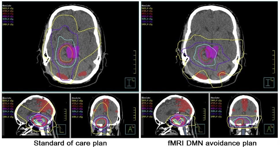
Isodose curves for a representative patient comparing dose distributions of the standard-of-care treatment plan and the fMRI default mode network avoidance plan. (Courtesy: C Rhodes et al J. Med Imaging Radiat. Sci. 10.1016/j.jmir.2018.09.003)
Radiation therapy is commonly employed as a primary or adjunct treatment for brain tumours. However, neurocognitive impairment after brain radiotherapy is a known problem that restricts its use. The ability to limit dose to brain regions associated with cognitive performance may help minimize treatment-related loss of cognitive functioning, ultimately improving patients’ long-term outcomes and quality-of-life.
Functional MRI (fMRI) provides a means to identify brain regions to selectively protect during radiotherapy. Previous research in this area has focused on task-based fMRI of language and sensory networks. Now, a team from University of Maryland School of Medicine has investigated the feasibility of incorporating resting-state fMRI data into radiation treatment plans for patients with primary brain tumours (J. Med Imaging Radiat. Sci. 10.1016/j.jmir.2018.09.003).
“Resting-state fMRI provides the ability to collect information on how the brain is functionally communicating without requiring the participant to perform a task, which he or she may be unable to do due to limited cognitive abilities or causing further fatigue to the ailing patient,” explains first author Chandler Rhodes. “Additional benefits include the ability to look at multiple brain networks (such as language, vision, hearing and memory) in a single 6–10 min scan, as well as the ability to collect this information on a standard MR scanner without the additional equipment needed for task-based fMRI.”
Seek and avoid
Rhodes and colleagues used resting-state fMRI to identify the brain’s default mode network (DMN), a set of cortical regions associated with cognitive functioning. Damage to this neural network can lead to reduced cognitive performance, and the researchers propose that protecting the DMN during radiation delivery could minimize side effects such as memory loss.
To investigate this premise, they retrospectively incorporated fMRI data from the DMN into the radiation treatment plans of nine patients with primary brain tumours. All patients had previously received standard-of-care radiotherapy using either intensity-modulated or 3D conformal radiotherapy.
For each participant, the researchers performed 3T MRI to obtain resting-state fMRI data and structural images. They overlaid the fMRI networks of the DMN onto each individual’s structural image, imported this into a treatment planning system and contoured the DMN onto the planning CT scan. Finally, they generated a second treatment plan that reduced dose to the DMN while maintaining dose to the planning target volume (PTV) and not increasing dose to organs-at-risk (OARs).
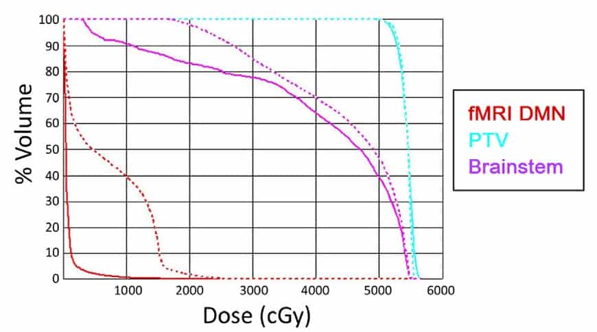
The team successfully extracted fMRI maps of the DMN and created DMN avoidance plans for all participants. In all cases, the new plans reduced the dose to brain areas related to cognitive functioning compared with the standard-of-care plans. On average, the avoidance plans reduced the maximum dose to the DMN by 12% and the mean dose by 20%.
Dose–volume histograms for a representative patient showing doses to the fMRI DMN, PTV and brainstem. The dashed line is the standard-of-care plan and the solid line is the fMRI DMN avoidance plan. (Courtesy: C Rhodes et al J. Med Imaging Radiat. Sci. 10.1016/j.jmir.2018.09.003)
Importantly, these dose reductions were achieved without compromising dose coverage of the PTV or significantly increasing dose to any of the OARs (brainstem, spinal cord, lenses, retina, lacrimal glands, cochlea, optic nerves and optic chiasm). The avoidance plan also reduced the dose non-PTV and non-OAR brain tissue.
Potential benefits
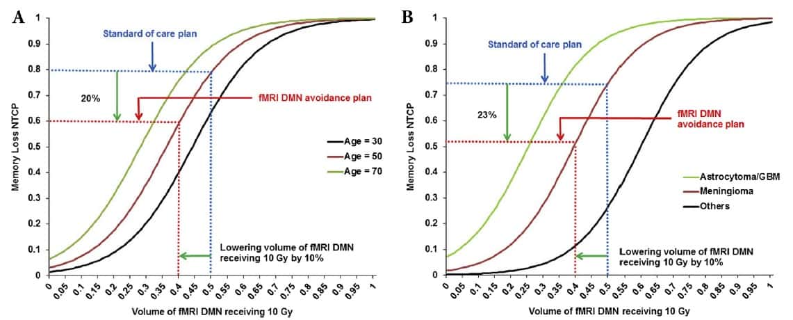
To estimate the relative benefit, in terms of improved cognitive function, for patients treated with the DMN avoidance plan, the team used a normal tissue complication probability (NTCP) modelling approach. Multivariate analysis showed that age, smoking history, tumour histology, and volume of DMN receiving 10 Gy (DNM10Gy) were all predictive of memory loss.
Using these variables, the researchers identified two logistic regression models that successfully predicted memory loss: one with age and DNM10Gy as variables; and the second with tumour histology and DNM10Gy as variables. Incorporating these two models into the NTCP calculation enabled them to calculate the probability of developing memory loss.
Estimated probability of memory loss using NTCP as a function of DNM10Gy with age (A) and tumour histology (B) as variables in the logistic regression models. (Courtesy: C Rhodes et al J. Med Imaging Radiat. Sci. 10.1016/j.jmir.2018.09.003)
On average, the fMRI DMN avoidance plan reduced the DNM10Gy from 50% to 40% compared with the standard-of-care plan. This dose reduction lowered the probability of developing memory loss by 20% for 50-year-old patients, for example, and by 23% for patients with meningioma.
The authors conclude that incorporating DMN derived from resting-state fMRI into radiation treatment plans is feasible and can reduce dose to the DMN without significantly affecting dose to the PTV or OARs. This approach may significantly reduce toxicity in brain regions associated with cognition.
They caution, however, that as the potential benefits were only estimated using models, the study does not prove that reducing dose to the DMN actually reduces the cognitive decline that often follows radiation treatment. They suggest that the clinical impact of this reduction in DMN dose needs to be further evaluated in a rigorous clinical trial.
The team also plans to test the proposed approach with proton therapy. “Since proton therapy has the potential to provide superior dose distribution in terms of sparing the fMRI DMN, our approach may demonstrate even more benefits with proton therapy,” says co-author Howard Zhang. “We are also planning a prospective study to assess the effectiveness of incorporating functional imaging into radiation therapy in terms of patient outcomes,” adds senior author Rao Gullapalli.
When Allied soldiers were evacuated from Dunkirk during the Second World War, the British military’s command centre for “Operation Dynamo” was located in secret tunnels under the White Cliffs of Dover. These days, such a huge logistical exercise would be inconceivable without the use of electronic devices, but back then the tunnels housed very little, if any, computer power. Even the Colossus computer, developed at Bletchley Park in Buckinghamshire to decipher German code messages, was primitive by today’s standards and occupied an entire set of rooms.
Fast forward to today and each of us carries around tiny communications devices with more computing power than was available to the entire British military intelligence in the Second World War. We drive cars with more computing power than the Apollo spacecraft that first landed men on the Moon. Desktop computers and laptops from only 20 years ago look Stone Age compared to today’s tablets, smart watches and phones given that so much electronics can be shoe-horned into a tiny space. Even TVs, washing machines and other household appliances are crammed with chips.
But what can we expect in the years ahead? Will we no longer need to carry our electronic devices wherever we go? Will we instead be able to wear them in our clothes or graft them onto our skin? The answers will depend on continuing advances in semiconductors – those hybrid materials that incorporate features of both insulators and conductors. What makes them the ultimate building block for electronic devices is that their conductivity can be switched on and off quickly and easily.
Hard limits: Wearable electronics are common today but still largely built around rigid objects based on 3D semiconductors. (Courtesy: iStock/filadendron)
The switching is possible because there’s an energy barrier between the low-energy valence band and the high-energy conduction band. Known as the band gap, electrons need to overcome this hurdle to flow through the material. All we have to do is apply an electric field to the semiconductor. A field of one polarity allows the charges to gain energy and progress through the material by crossing the band gap. Reverse the field and the electrons will lose energy, stay in the valence band and travel less.
This switching ability has allowed semiconductors to be fashioned into diodes – devices that let current flow in one direction but not the other – and into capacitors, which together form the building blocks of most modern electronic components. Combining two diodes and a metal-oxide semiconductor (MOS) capacitor, for example, gives you a field-effect transistor (FET), which in turn can be combined with other transistors into logic gates for computing.
These days, most FETs are made from 3D, bulk semiconductors, such as silicon or gallium arsenide, shaped into nanometric-scale structures using advanced material-processing techniques. Such transistors are hugely efficient – they’re the backbone of modern electronics – but they are rigid and opaque and so can’t easily be incorporated into clothes or paper. Fortunately, there is a new kid on the block that could lead to more versatile devices, such as health-monitoring patches that can be worn on the skin, smartphones woven into jumpers or solar panels incorporated into your backpack to charge your phone.
Soft future: Wearable electronic devices based on 2D semiconductors could lead to new applications in everything from medicine to consumer goods. (Courtesy: iStock/metamorworks)
Slimmed down
These materials are layered semiconductors, in which bulk 3D solids have been thinned down to essentially 2D slivers just a few atoms thick. This slimming process can be done using simple approaches such as the “Scotch-tape” method that Andre Geim and Kostya Novoselov developed to isolate graphene from graphite in their 2010 Nobel-prize-winning work. Other methods include “shear exfoliation” in a liquid medium using an industrial-grade blender to produce semiconductor inks and films, as well as chemical techniques, in which the material is grown by depositing vapours on a target substrate.
2D semiconductors are transparent and flexible, offering extra functionality for novel gadgets
Being 2D, these new semiconductors are transparent and flexible, allowing them to be incorporated into electronic devices with extra functionality for novel gadgets such as flexible memory devices and transparent photodetectors. But replacing traditional 3D semiconductors with atom-thick structures as the active components in transistors is not straightforward. One difficulty arises when these new materials are connected to metal electrodes, which are used as links to carry current from one component to another.
With a 2D semiconductor, the entire device is effectively a surface. So when it’s connected to a metal, differences in the “work functions” between the two materials create an energy barrier at the interface. Known as a “Schottky barrier”, it can be overcome in 3D semiconductors by chemically doping the semiconductor near the interface with the metal. However, in 2D semiconductors doping is not an option as foreign species can drastically change the material’s physical properties.
Another problem with 2D semiconductors is that their conductivity is heavily influenced by annoying states that form in the energy barrier at the surface of the crystal. These “surface states”, which arise because the crystal periodicity ends at the surface, cannot contribute to conduction. In fact, electrons get trapped in these states, cutting the conductivity of the material by an amount that depends on the number of traps.
These surface states do three things. First, they immobilize conduction electrons, reducing their density and the current flow. Second, the trapped electrons scatter mobile electrons, reducing their movement and raising the resistance of the semiconductor “channel” between the two metal contacts. Third, the states form a layer of surface charge that alters the semiconductor’s capacitance, making it harder for an external electric field to enter the material and less likely for the field to induce a current flow.
Figure 1: Sticky tape semiconductor
Surface states, in other words, sound like bad news for 2D semiconductors. To explore how they hinder conduction, we’ve carried out experiments on field-effect transistors made from molybdenum ditelluride (MoTe2), which has a band gap similar to that of silicon and is easy to turn into thin layers. We built the transistors using tape to pull off nanometre-thin flakes of MoTe2 from a bulk crystal and then transferring them onto a highly doped silicon substrate. The substrate acts as the transistor’s gate electrode, while its oxide layer serves as the gate dielectric. We then patterned metal contacts onto the semiconductor flake (figure 1).
Surprise, surprise
We did two separate investigations into how these 2D devices conduct. For the first project, we investigated the Schottky barriers that form between various metals and the MoTe2 channel at cryogenic temperatures below 80 K (2D Mater.5 025023). We particularly wanted to measure the height of the barrier because we could then see if changing it made it any easier or harder for charges to enter the channel, which could let us use the transistors as a memory device.
Our hypothesis was that we’d be able to study how the height of the barrier affects conduction by changing the metal electrode. But as so often happens in experimental physics, we uncovered two unexpected results. At the low temperatures we were working at, the nominal thermal energy that allows electrons to overcome the energy barrier and conduct is absent, effectively “freezing” the carriers in their ground state. We therefore doubted that a transistor made from MoTe2 could switch on and conduct current.
However, we found that it switched on and off even at temperatures as low as 300 mK. Indeed, the device showed all the response characteristics of a “Schottky diode” – a device formed by putting a semiconductor in contact with a metal, rather than by changing the doping in it. We confirmed this finding by quantifying the tiny change in Schottky-barrier height as the metal was altered. Although previous studies into similar materials had shown similar results, it was exciting to see the same trend in a novel material at low temperatures. The result boosted our confidence in our findings and encouraged us to go further.
Our second surprising result was how charge gets over the energy barrier into the channel. This usually happens in one of three ways. There’s thermionic emission (like jumping over a barrier); there’s diffusion (like “trickling” over a barrier); and then there’s tunnelling (digging through a barrier). Sometimes, it’s a combination of all three. At low temperatures, tunnelling is usually the dominant mechanism since electrons should not have enough energy to jump over the barrier. But to our amazement, we found that thermionic emission is the main method of charge injection.
To estimate the Schottky barrier height, we then set up an experiment in which we altered the voltage between the two metal contacts (the source and drain electrodes) and then read off the source-drain current. Working at temperatures from 80 K down to 40 K, we calculated that the barrier height ranged from 10 meV for palladium contacts up to 50 meV for titanium. With the difference in metal work function being much larger, it became clear that modulating the Schottky barrier height was not going to be a straightforward task.
Over the threshold
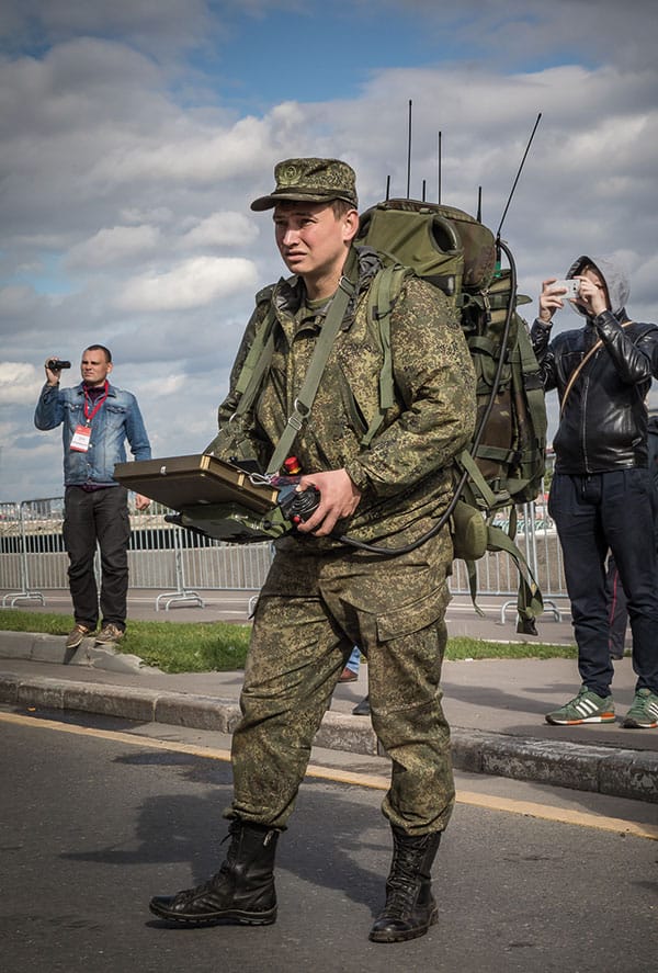
He ain’t heavy: Flexible, lightweight electronic devices based on 2D semiconductors could benefit soldiers who would have less kit to carry around. (Courtesy: Shutterstock/Naletova Elena)
Our second project involved probing the nature of charge “traps”. These occur in places in the semiconducting channel where the periodicity of the lattice is broken, confining electrons and raising the resistance at that point (Adv. Mater.29 1605598). But when we swept the gate bias from a voltage that hinders conduction through the FET (an “off” state) to a voltage that lets a current through (“on”) and then back again, we found something unusual. The size of the current was not the same in the two directions. Instead, there was a hysteresis.
When the FET is switched on, the charge traps capture electrons. But when it’s turned off, the electrons are emitted, reducing the measured current. The capture and emission of the electrons is a time-dependent process, which leads to the appearance of “transient” currents that last much longer than in bulk semiconductors. These are currents that change with time while recording the gate sweeps.
In fact, we observed two different transient currents that could stem from trapped charges. There are emission currents, which do not vary in size with the applied voltage. Then there are currents that increase linearly with voltage and so conform to Ohm’s law. The latter currents, which never occur in bulk semiconductors, alter the minimum voltage needed to turn the FET on. We coined them “threshold transients” and, to our surprise, they account for most of the hysteresis in these systems.
Fast forward
These kinds of experiments, which probe the basic physical mechanisms underpinning novel 2D devices, offer a way to control their conductance and create new kinds of electronic devices. By understanding Schottky barriers, for example, we could devise photodetectors in which incoming photons have enough energy to excite charges in the semiconductor and jump over the barrier – but not enough to move from the valance to the conduction band. Based on the barrier heights we found in our MoTe2 devices, this material could be used to detect infrared light, making it perfect for thermal imaging in harsh conditions, such as when it’s foggy or the air is full of smoke from fires.
Semiconducting devices based on novel 2D materials that are transparent and flexible will also be of huge benefit for wearable electronics. Graphene has already been successfully incorporated onto fibres (Sci. Rep.7 4250), but other materials could allow textiles to carry computing power or even energy storage, replacing bulky batteries. By reducing the energy requirements and physical size of sensors and computational devices, the next generation of wearable electronics could transform life for scientists on remote expeditions or for soldiers out in the field. The contrast with the computers used back in the Second World War could not be more extreme.
Expected to cost tens of billions of euros, the ITER fusion reactor aims to show that it is technically feasible to get usable amounts of energy from a controlled fusion reaction. The project has, however, been hit by numerous delays and the first plasma is not expected until at least 2025 at the earliest. The first experiments using a “burning” fusion fuel – a mixture of deuterium and tritium – will not begin until the mid 2030s with the facility aiming to generate 500 MW of power. ITER’s rapidly increasing budget has also led to frequent – although so far unsuccessful — efforts by the US Senate to withdraw from it.
The sword of Damocles
The NASEM report, issued in late December, builds on an interim version published in early 2018 that warned of the consequences of leaving ITER. The latest version states that ITER is the “only existing project expected to create and study a burning plasma [being] the next critical step in the development of fusion energy”. Yet the report also indicates that the US needs its own complementary fusion programme. Without it, says panel co-chair Melvyn Shochet, a physicist at the University of Chicago, “the US risks being overtaken by other countries that are ramping up their science and technology”.
The report imagines a compact pilot plant capable of producing a similar power to ITER in a device much smaller in size and cost. Knowledge obtained from such a device, it asserts, would be sufficient to design the first commercial fusion power systems. “The programme management strategy for the coming decades would benefit from exploiting the benefits of US ITER participation as a full partner, while advancing a coordinated domestic research program directed at elements of a fusion power system not addressed by ITER,” the authors state.
However, the project will need an extra $200m every year in government funding for fusion over several decades, which given tight government budgets could cause problems. “There’s a sword of Damocles hanging over all discretionary expenditures, including scientific research,” says former plasma physicist Rush Holt, who is now chief executive of the American Association for the Advancement of Science. On the other hand, Holt adds, “some of the new fusion approaches that might bear fruit are being conducted without or with little federal funding, such as at TAE Technologies and the high-field approach with superconducting tape [developed at the Massachusetts Institute of Technology].”
Fusion energy goals
James Van Dam, acting associate director for fusion energy sciences in the Department of Energy (DOE), told Physics World that he welcomes the report’s “thoughtful recommendations” adding that they will be useful to the DOE as it has recently launched a “long-term strategic planning effort” in fusion. “[The report] says it’s time to get back to harnessing practical fusion energy,” he adds.
The report has also earned positive reviews from members of the private fusion community, including Jeff Quintenz, energy group vice president of General Atomics. “We are particularly pleased with the committee’s endorsement of US participation in the ITER project and its recommended strategy to pivot the US programme toward a fusion energy goal in the intermediate term,” he says.
The practical transmission of single photons over a record-breaking distance of 20,000 km has been demonstrated between satellites in Earth orbit and a ground station in Italy. This was achieved by researchers led by Paolo Villoresi at the University of Padua, who say that the exchange confirms that satellite quantum communications are feasible on a global scale.
Global Navigation Satellite Systems (GNSSs) consist of constellations of satellites that broadcast timing signals to a ground-based receiver such as a mobile phone or vehicle navigation system. Several nations have constructed their own GNSSs, each with their own satellite constellations orbiting Earth at distances of 19,000-36,000 km.
These systems operate using microwaves at about 1 GHz, which means that a GNSS signal can easily be disrupted or intercepted by malicious third parties. This is a problem because GNSS’s are of crucial importance to the economic and military security of the nations that deploy them.
Quantum keys
Quantum communications uses single photons and offers a way of achieving secure and robust communications – both between satellites and between satellites and receivers on the ground. A well-established technique called quantum key distribution (QKD), for example, could be used to encrypt GNSS and other signals.
Quantum techniques involve the exchange of single photons, which has already been demonstrated for satellites that are relatively close to Earth. In 2016, Villoresi and colleagues achieved a transmission distance of 7000 km. The following year, physicists in China and Austria used a satellite to achieve QKD over a distance of 7400 km between Beijing and Vienna.
Longer communication
GNSS and other satellites at 19,000-36,000 km move slower relative to Earth’s surface than the satellites at lower orbits that were used in previous quantum demonstrations. As a result, such satellites can communicate for longer with individual grounds stations and are therefore better suited for creating quantum communications networks. However, exchanging single photons over these distances remains a challenge.
Villoresi’s team did their demonstration using the arrays of retroreflectors that are mounted on Russia’s GLONASS GNSS satellites. Working at the Italian Space Agency’s Matera Laser Ranging Observatory (MLRO), the researchers fired a train of laser pulses towards two GLONASS satellites. The light was then reflected back to the MLRO and collected by a single-photon detector.
By estimating the losses in the communication channel, the researchers were able to confirm that existing technology could deployed on satellites to generate key-carrying single photons. In future studies, they will develop active sources of QKD photons to be placed on-board GNSS satellites.
A European spacecraft launched in October 2017 provides data on worldwide tropospheric pollution to a finer degree than ever before, even though it’s not yet fully operational. Part of the European Space Agency’s (ESA) Copernicus Earth Observation programme, the Sentinel 5 Precursor (S5P) carries the Dutch-built TROPOspheric Monitoring Instrument (TROPOMI), a four-band spectrometer.
S5P flies in a near polar orbit at an altitude of 824 km; it scans the entire globe each day. The principal investigator for TROPOMI, Pepijn Veefkind of the Royal Netherlands Meteorological Institute (KNMI), presented maps pinpointing the source of several important pollutants, as identified by TROPOMI, to journalists at the American Geophysical Union’s (AGU) Fall Meeting in December in Washington, DC.
Nitrogen dioxide (NO2) is produced, for example, by power plants and forest fires, but has a lifetime of only a day. “There is more detailed information than we ever had” on the specific location of NO2 emissions, thanks to the daily fly-bys and high resolution of TROPOMI images, Veefkind said. “You can go from the global view, zoom all the way in to the urban regions”, which is what the instrument was designed to do.
Veefkind showed a NASA Suomi-NPP Visible Infrared Imaging Radiometer Suite (VIIRS) image of a massive smoke plume, several hundred kilometres long, from the Camp Fire that obliterated Paradise, California, starting on November 8, 2018. He overlaid NO2 data from TROPOMI, collected just five minutes later, onto the VIIRS image, to show that the fire was extremely hot and that the biomass was burning incompletely.
Carbon monoxide (CO) is produced by incomplete burning, especially of biomass, such as by wildfires, Veefkind said, and is well tracked by TROPOMI. CO lives longer than NO2, so its plume can be traced from source regions through the entire hemisphere for the first time. Its presence is strong in TROPOMI images of the Camp Fire. Similarly, TROPOMI also revealed that the carcinogenic pollutant formaldehyde (HCHO) was strongly present in the fire’s plume.
In the future TROPOMI will provide detailed information on the formation of tropospheric methane (CH4), a powerful greenhouse gas. It will rely on VIIRS images to find areas that are completely cloud-free, a necessity for accurate methane tracking.
S5P flies in almost the same polar orbit as NASA’s Suomi NPP, which was launched in 2011. Designed to work in tandem with the NASA satellite, S5P passes over each spot on Earth five minutes later. The VIIRS hyperspectral instrument, although an older technology with lower resolution than TROPOMI, covers a similar swath on Earth’s surface, said Barry Lefer, program manager of NASA’s tropospheric composition programme. ESA’s Claus Zehner agreed that the two satellites are powerful partners in providing air quality data to European environmental protection agencies.