Smartphones, tablets and laptops are stacked with computing power, but they’re mostly rigid, inflexible objects. Semiconductors that have been shrunk from 3D to 2D could, however, lead to flexible, wearable electronic devices, as Nicola Townsend and Iddo Amit explain

When Allied soldiers were evacuated from Dunkirk during the Second World War, the British military’s command centre for “Operation Dynamo” was located in secret tunnels under the White Cliffs of Dover. These days, such a huge logistical exercise would be inconceivable without the use of electronic devices, but back then the tunnels housed very little, if any, computer power. Even the Colossus computer, developed at Bletchley Park in Buckinghamshire to decipher German code messages, was primitive by today’s standards and occupied an entire set of rooms.
Fast forward to today and each of us carries around tiny communications devices with more computing power than was available to the entire British military intelligence in the Second World War. We drive cars with more computing power than the Apollo spacecraft that first landed men on the Moon. Desktop computers and laptops from only 20 years ago look Stone Age compared to today’s tablets, smart watches and phones given that so much electronics can be shoe-horned into a tiny space. Even TVs, washing machines and other household appliances are crammed with chips.
But what can we expect in the years ahead? Will we no longer need to carry our electronic devices wherever we go? Will we instead be able to wear them in our clothes or graft them onto our skin? The answers will depend on continuing advances in semiconductors – those hybrid materials that incorporate features of both insulators and conductors. What makes them the ultimate building block for electronic devices is that their conductivity can be switched on and off quickly and easily.

The switching is possible because there’s an energy barrier between the low-energy valence band and the high-energy conduction band. Known as the band gap, electrons need to overcome this hurdle to flow through the material. All we have to do is apply an electric field to the semiconductor. A field of one polarity allows the charges to gain energy and progress through the material by crossing the band gap. Reverse the field and the electrons will lose energy, stay in the valence band and travel less.
This switching ability has allowed semiconductors to be fashioned into diodes – devices that let current flow in one direction but not the other – and into capacitors, which together form the building blocks of most modern electronic components. Combining two diodes and a metal-oxide semiconductor (MOS) capacitor, for example, gives you a field-effect transistor (FET), which in turn can be combined with other transistors into logic gates for computing.
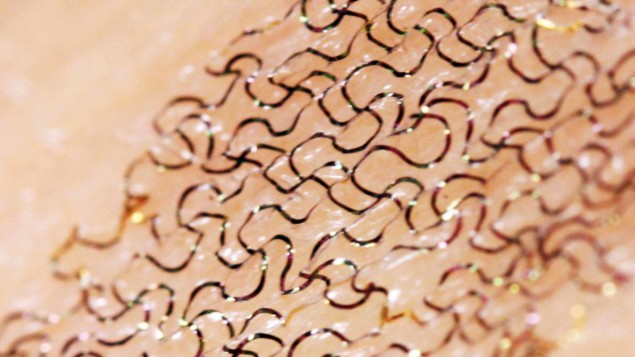
These days, most FETs are made from 3D, bulk semiconductors, such as silicon or gallium arsenide, shaped into nanometric-scale structures using advanced material-processing techniques. Such transistors are hugely efficient – they’re the backbone of modern electronics – but they are rigid and opaque and so can’t easily be incorporated into clothes or paper. Fortunately, there is a new kid on the block that could lead to more versatile devices, such as health-monitoring patches that can be worn on the skin, smartphones woven into jumpers or solar panels incorporated into your backpack to charge your phone.

Slimmed down
These materials are layered semiconductors, in which bulk 3D solids have been thinned down to essentially 2D slivers just a few atoms thick. This slimming process can be done using simple approaches such as the “Scotch-tape” method that Andre Geim and Kostya Novoselov developed to isolate graphene from graphite in their 2010 Nobel-prize-winning work. Other methods include “shear exfoliation” in a liquid medium using an industrial-grade blender to produce semiconductor inks and films, as well as chemical techniques, in which the material is grown by depositing vapours on a target substrate.
2D semiconductors are transparent and flexible, offering extra functionality for novel gadgets
Being 2D, these new semiconductors are transparent and flexible, allowing them to be incorporated into electronic devices with extra functionality for novel gadgets such as flexible memory devices and transparent photodetectors. But replacing traditional 3D semiconductors with atom-thick structures as the active components in transistors is not straightforward. One difficulty arises when these new materials are connected to metal electrodes, which are used as links to carry current from one component to another.
With a 2D semiconductor, the entire device is effectively a surface. So when it’s connected to a metal, differences in the “work functions” between the two materials create an energy barrier at the interface. Known as a “Schottky barrier”, it can be overcome in 3D semiconductors by chemically doping the semiconductor near the interface with the metal. However, in 2D semiconductors doping is not an option as foreign species can drastically change the material’s physical properties.
Another problem with 2D semiconductors is that their conductivity is heavily influenced by annoying states that form in the energy barrier at the surface of the crystal. These “surface states”, which arise because the crystal periodicity ends at the surface, cannot contribute to conduction. In fact, electrons get trapped in these states, cutting the conductivity of the material by an amount that depends on the number of traps.
These surface states do three things. First, they immobilize conduction electrons, reducing their density and the current flow. Second, the trapped electrons scatter mobile electrons, reducing their movement and raising the resistance of the semiconductor “channel” between the two metal contacts. Third, the states form a layer of surface charge that alters the semiconductor’s capacitance, making it harder for an external electric field to enter the material and less likely for the field to induce a current flow.

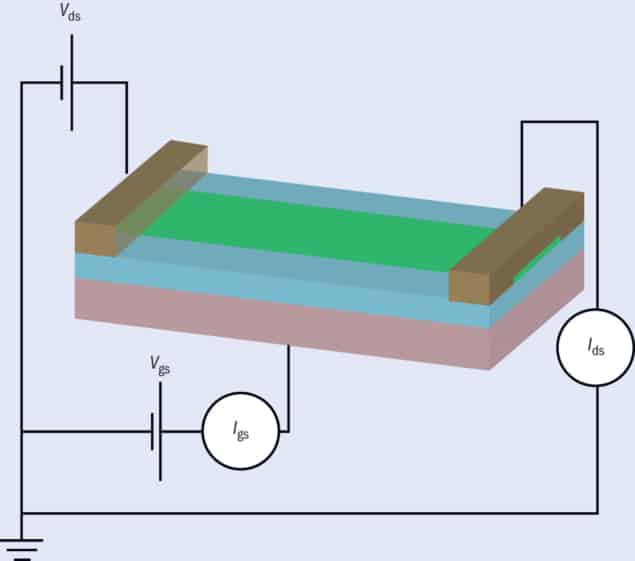
Surface states, in other words, sound like bad news for 2D semiconductors. To explore how they hinder conduction, we’ve carried out experiments on field-effect transistors made from molybdenum ditelluride (MoTe2), which has a band gap similar to that of silicon and is easy to turn into thin layers. We built the transistors using tape to pull off nanometre-thin flakes of MoTe2 from a bulk crystal and then transferring them onto a highly doped silicon substrate. The substrate acts as the transistor’s gate electrode, while its oxide layer serves as the gate dielectric. We then patterned metal contacts onto the semiconductor flake (figure 1).
Surprise, surprise
We did two separate investigations into how these 2D devices conduct. For the first project, we investigated the Schottky barriers that form between various metals and the MoTe2 channel at cryogenic temperatures below 80 K (2D Mater. 5 025023). We particularly wanted to measure the height of the barrier because we could then see if changing it made it any easier or harder for charges to enter the channel, which could let us use the transistors as a memory device.
Our hypothesis was that we’d be able to study how the height of the barrier affects conduction by changing the metal electrode. But as so often happens in experimental physics, we uncovered two unexpected results. At the low temperatures we were working at, the nominal thermal energy that allows electrons to overcome the energy barrier and conduct is absent, effectively “freezing” the carriers in their ground state. We therefore doubted that a transistor made from MoTe2 could switch on and conduct current.
However, we found that it switched on and off even at temperatures as low as 300 mK. Indeed, the device showed all the response characteristics of a “Schottky diode” – a device formed by putting a semiconductor in contact with a metal, rather than by changing the doping in it. We confirmed this finding by quantifying the tiny change in Schottky-barrier height as the metal was altered. Although previous studies into similar materials had shown similar results, it was exciting to see the same trend in a novel material at low temperatures. The result boosted our confidence in our findings and encouraged us to go further.
Our second surprising result was how charge gets over the energy barrier into the channel. This usually happens in one of three ways. There’s thermionic emission (like jumping over a barrier); there’s diffusion (like “trickling” over a barrier); and then there’s tunnelling (digging through a barrier). Sometimes, it’s a combination of all three. At low temperatures, tunnelling is usually the dominant mechanism since electrons should not have enough energy to jump over the barrier. But to our amazement, we found that thermionic emission is the main method of charge injection.
To estimate the Schottky barrier height, we then set up an experiment in which we altered the voltage between the two metal contacts (the source and drain electrodes) and then read off the source-drain current. Working at temperatures from 80 K down to 40 K, we calculated that the barrier height ranged from 10 meV for palladium contacts up to 50 meV for titanium. With the difference in metal work function being much larger, it became clear that modulating the Schottky barrier height was not going to be a straightforward task.
Over the threshold

Our second project involved probing the nature of charge “traps”. These occur in places in the semiconducting channel where the periodicity of the lattice is broken, confining electrons and raising the resistance at that point (Adv. Mater. 29 1605598). But when we swept the gate bias from a voltage that hinders conduction through the FET (an “off” state) to a voltage that lets a current through (“on”) and then back again, we found something unusual. The size of the current was not the same in the two directions. Instead, there was a hysteresis.
When the FET is switched on, the charge traps capture electrons. But when it’s turned off, the electrons are emitted, reducing the measured current. The capture and emission of the electrons is a time-dependent process, which leads to the appearance of “transient” currents that last much longer than in bulk semiconductors. These are currents that change with time while recording the gate sweeps.
In fact, we observed two different transient currents that could stem from trapped charges. There are emission currents, which do not vary in size with the applied voltage. Then there are currents that increase linearly with voltage and so conform to Ohm’s law. The latter currents, which never occur in bulk semiconductors, alter the minimum voltage needed to turn the FET on. We coined them “threshold transients” and, to our surprise, they account for most of the hysteresis in these systems.
Fast forward
These kinds of experiments, which probe the basic physical mechanisms underpinning novel 2D devices, offer a way to control their conductance and create new kinds of electronic devices. By understanding Schottky barriers, for example, we could devise photodetectors in which incoming photons have enough energy to excite charges in the semiconductor and jump over the barrier – but not enough to move from the valance to the conduction band. Based on the barrier heights we found in our MoTe2 devices, this material could be used to detect infrared light, making it perfect for thermal imaging in harsh conditions, such as when it’s foggy or the air is full of smoke from fires.
Semiconducting devices based on novel 2D materials that are transparent and flexible will also be of huge benefit for wearable electronics. Graphene has already been successfully incorporated onto fibres (Sci. Rep. 7 4250), but other materials could allow textiles to carry computing power or even energy storage, replacing bulky batteries. By reducing the energy requirements and physical size of sensors and computational devices, the next generation of wearable electronics could transform life for scientists on remote expeditions or for soldiers out in the field. The contrast with the computers used back in the Second World War could not be more extreme.


