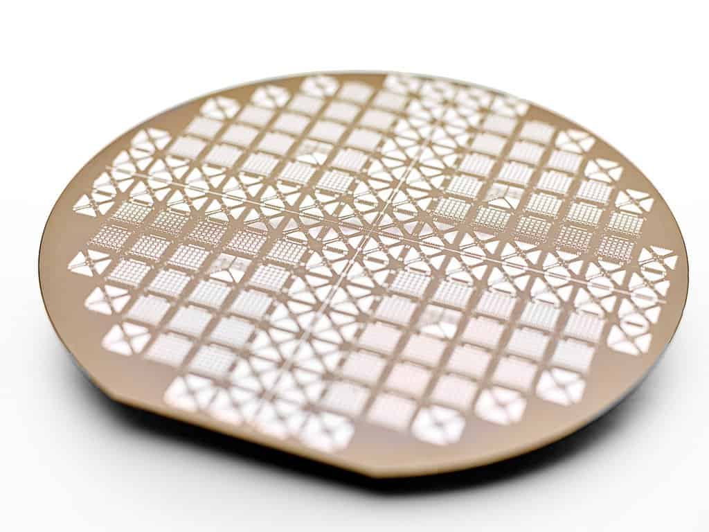
Innovation: patent applications review

A round-up of some recent international patent applications in radiation therapy.

Silicon photomultipliers line up for Cerenkov-guided radiotherapy

Cerenkov emission during external-beam radiotherapy provides a useful quality assurance tool and potential for online tracking of tumours during treatment. However, molecular probing of the cancer status during delivery has not been developed — mainly due to the limited sensitivity of current photodetectors for Cerenkov emission and a lack of tools to fit into the complex treatment delivery environment. Silicon photomultipliers (SiPMs) offer the high sensitivity of photomultiplier tubes, with a similar a form factor to silicon photodiodes, allowing for improved flexibility in device design. In patent application WO/2018/208775, University of Michigan researchers present a SiPM array-based multispectral optical probe. They assess the feasibility of using SiPMs to detect Cerenkov emission and interrogate physiological information during radiotherapy.

Dose calculations compensate for inhomogeneous tissue

Particle therapy of inhomogeneous tissues such as lungs, which include an irregular pattern of air cavities, is difficult as the structure of such tissue affects the trajectory of the ions and can cause errors. Raysearch Laboratories has developed ion radiotherapy dose calculations that compensate for tissue in which voxels may be inhomogeneous in density, by approximating a portion of the voxel as an air cavity (WO/2018/189364). Each dose voxel is inscribed in a 3D grid comprising a number of cells, preferably in such a way that the voxel overlaps at least one cell fully. Each cell comprises one portion representing the density of tissue and a second representing the density of air, the first and second portions forming a cell pattern. The propagation of ions through the voxel is then calculated based on the cell pattern in any cells overlapping the voxel.

Compact system delivers gantry-less particle therapy

A team from Massachusetts General Hospital has published details of a gantry-less particle therapy system (WO/2018/204579). The described methods can be used to treat patients in the same room as the particle therapy system by positioning the treatment area inward from the system’s beam track. Charged particles are extracted from an ion source and accelerated in a beam transport system. This transport system has an annular portion that extends in one plane and circumscribes a volume, an arcuate portion in a second plane, and a transition portion that connects the two. The arcuate portion terminates at a beam nozzle that extends radially inward from the annular portion to deliver an ion beam to a treatment area within the volume defined by the annular portion.

Motion target volume accounts for shape changes

Elekta has devised a way to generate a motion target volume that represents changes in the shape of the target in a patient during radiotherapy delivery (WO/2018/208390). At least one computer system is configured to receive a series of medical images that include the target region, with each image taken at a different time point. The computer defines a 3D volume containing the target in each image; this 3D volume may be different in at least two of the images due to differences in the shape of the target region. The system then co-registers the 3D volumes and generates the motion target volume, which encompasses each of the 3D volumes.

Dermatology system delivers fast skin treatments

Sensus Healthcare has invented a dermatological radiotherapy system with a hybrid imager that can be used to diagnose, treat and verify treatment of skin cancers or lesions (WO/2018/187619). The system provides a means to deliver the required radiation dose to the patient in a significantly shorter period of time — for example, less than 1 min as opposed to more than 5 min — by increasing the flow of photons emitted from a radiotherapy treatment device. This is achieved by shortening the removable applicator of the radiotherapy device, and using either relatively thick filters with normal dose rates (less than 1000 cGy/min), or thin filters with relatively high dose rates (above 1000 cGy/min).

Quantum tech investments and visiting the Francis Crick Institute

In this episode of Physics World Weekly, Physics World’s general physics editor Hamish Johnston is joined by colleagues to discuss quantum technologies, biomedical research plus the week’s research highlights.

First up in the podcast, industry Editor Margaret Harris speaks about the launch of the €1bn European Quantum Flagship, which she attended at the Hofburg palace in Vienna, Austria. Harris was also at a showcase event in London about the UK’s national quantum technology initiative, which has been allocated extra funding in the government’s recent budget.

Later in the podcast, Physics World editor Matin Durrani discusses his recent visit to the Francis Crick Institute. Opened in 2016 in the King’s Cross district of London, the research centre is focussed on the fundamental biology underlying health and disease. Along the way, you will hear from the researchers Paul Bates and Esther Wershof who apply principles of maths and physics to modelling biomolecular systems.

If you enjoy what you hear, then you can subscribe via the Apple podcast app or your chosen podcast host.

The value of sorting graphene flakes from fakes

Researchers from the NUS Centre for Advanced 2D Materials examining the quality of graphene samples. Credit: National University of Singapore

While theories abound to explain the lag between investment and commercial return in graphene research, a supply chain flooded with samples of graphite masquerading as graphene certainly won’t help. Yet when researchers at the National University of Singapore systematically analysed samples from over 60 suppliers based in America, Asia and Europe, they found most contained less 10% of what the International Standardization Organization defines as graphene, with just one sample containing more than 40% high-quality graphene, as reported in Advanced Materials.

“It is alarming to uncover that producers are labelling black powders as graphene and selling them for top dollar, while in reality, they contain mostly cheap graphite,” says Antonio Castro Neto, Director of the NUS Centre for Advanced 2D Materials, who led the study. “There is a strong need to set up stringent standards for graphene characterization and production to create a healthy and reliable graphene market worldwide.”

Suffering from a few too many

The miraculous properties of graphene have attracted headlines ever since the material was isolated and characterized by Kostya Novoselov and Andre Geim, who were awarded a Nobel Prize for the work in 2010. Strictly speaking graphene is a single layer of carbon atoms arranged in a honeycomb like lattice, but “few-layer” graphene can retain much of the fascinating alliance of extraordinary electrical and mechanical properties. However when the number of layers starts to number more than just a few, the wonder material behaves less and less like graphene and more and more like graphite, also known as pencil lead.

The importance of distinguishing graphene from graphite has been recognized for several years, prompting the International Standardization Organization to set a precise definition for what can be defined as graphene – fewer than 10 layers. While this clarifies things for patent attorneys, a definition is little use to the graphene sector if suppliers continue to supply graphite in place of graphene, and users lack the resources to distinguish graphene flakes from graphene fakes.

“Whether producers of the counterfeit graphene are aware of the poor quality is unclear,” says Neto. “Regardless, the lack of standards for graphene production gives rise to bad quality of the material sold in the open market. This has been stalling the development of the future applications.”

The results of the NUS study come just months after the establishment of the Graphene Service in the UK, a collaboration between the National Physical  Laboratory in Teddington and the National Graphene Institute at the University of Manchester. The Graphene Service aims to leverage the expertise in the two institutions to characterize samples for users and provide advice on their potential uses.

Graphenea launches a graphene foundry service to manufacture custom circuit designs on graphene wafers up to 6”. Credit: Graphenea

Evaluating foundry solutions

In Europe investment in graphene to the tune of €1 billion in the form of the Graphene Flagship has set an unprecedented high bar on expectations for the material’s worth. While little research is possible without funding, funding alone is little guarantee of commercially successful research, and the difficulty of the task should not be ignored when questioning the time taken to cash in on graphene research investments. With a view to easing at least one stage of the process, Graphene Flagship partner Graphenea have now released the Graphene Foundry service, aimed at “enabling fast device prototyping and accelerating development of new applications, lowering entry barriers to graphene-based solutions.”

The foundry offers to manufacture custom circuit designs on graphene wafers up to 6” and promises stringent quality control on all of its samples using Raman spectroscopy, optical microscopy and electrical tests. While you can bag a Grapehenea field effect transistor device at $385, a 4” wafer could set you back $7,950.00. Given the value placed on the graphene market once its true potential is unleashed, some might say an option that side-steps the pencil peddlers and other fabrication pitfalls would be cheap at twice the price.

Turbulence causes swimming algae to congregate in dense patches, say physicists

Mild turbulence on the millimetre scale causes swimming phytoplankton to form dense patches, according to researchers in Germany and the UK. The research could boost our understanding of the spatial distribution of phytoplankton in oceans and lakes and help predict – and possibly prevent — the occurrence of toxic algal blooms.

Phytoplankton are microscopic algae that live near the surface of oceans and lakes. Some phytoplankton are motile, which means that they can propel themselves forwards. Like plants, they derive energy from the Sun by photosynthesis and produce more than 50% of oxygen we breathe. The organisms also play a key role in regulating atmospheric carbon dioxide levels.

An algal bloom is created when environmental factors such as nutrient availability and water temperature are favourable for the rapid reproduction of algae. Blooms can be destructive to wildlife, fisheries and tourism by blocking sunlight and by the release of toxic compounds into the water by the algae.

Mixing effect

Blooms can stretch over hundreds of square kilometres of ocean. Tidal currents and winds will often create uneven spatial distributions of algae, resulting in kilometre-sized patches. At length scales shorter than a centimetre, the mixing effect of fluid turbulence was expected to result in a uniform density of microorganisms. However, recent observations surprised scientists by showing that algal blooms have patchy distributions even at the millimetre scale. This patchiness could affect how fast a bloom develops because phytoplankton can reproduce sexually and therefore reproduction rates could be higher in regions of high density.

“The fact that there is a patchy distribution of phytoplankton on a kilometre scale can be easily understood and explained by oceanic currents and strong winds. Nevertheless, at the small scale, hydrodynamics should make things very homogeneous. And yet it doesn’t,” explains Marco Mazza, of Loughborough University.

Mazza and colleagues at Loughborough and the Max Planck Institute for Dynamics and Self-Organization in Göttingen used computer simulations and calculations to explore the origins of this unexpected millimetre-scale patchiness. They have shown that that an interplay between phytoplankton motility and interactions between individual organisms could play a role in creating patchiness on short length scales.

Navier–Stokes equations

The team looked at how motile phytoplankton are affected by hydrodynamic flows. To assess the phytoplankton behaviour on a sub-centimetre scale, the researchers combined 3D particle dynamics simulations with Navier–Stokes equations. The latter are the governing equations of fluid flows and define the relationship between the pressure, temperature, density, and velocity.

“We are solving the full Navier–Stokes equations without any further approximations and coupling this to a particle model describing the position of the particle within the flow, speed and direction of its swimming, it’s orientation, and thermal and biological noise,” Mazza explains, adding “Moreover, we consider the particle-particle interactions”.

Researchers found that the coupling of interactions between individuals to the small-scale flow features strongly favours the creation of dense patches of the organisms.

Prediction tool

These patches have implications to ecology and even human health, as algae will be more likely to mate in dense areas, leading to even faster growth. This research could ultimately contribute to creation of a tool for predicting algal blooms, which would be very useful to those involved in fishing and tourism.

“We are doing fundamental physical research and bridging the research to biology is a challenge,” says Michael Wilczek at the Max Planck Institute. For example, what we did not include in our study at all is population dynamics. Another interesting future step would be to include the shapes and sizes of the individual phytoplankton species. Alternatively, we could extend these studies to include zooplankton, where small scale patchiness is even more important, since zooplankton wants to prey on phytoplankton.”

Raymond Goldstein of the University of Cambridge, who was not involved in the work, told Physics World “the general issue is extremely interesting, but I don’t think the researchers have yet explained exactly the mechanism by which the clustering occurs. I do not see a clear physical picture of what exactly the interactions and alignments of cell are that lead to cluster formation. Having said that, this [research] will certainly motivate further investigations, precisely because it raises a nice set of questions and a way to analyse them.”

The research is reported in Proceedings of the National Academy of Sciences.

Are our water vapour emissions warming the climate?

Plain old H2O: the most abundant and powerful greenhouse gas in the Earth’s atmosphere. Water vapour accounts for around half the present-day greenhouse effect and without it our planet would probably be frozen and lifeless. But should we worry about adding more, given that temperatures are rising? A new study reveals that as long as our water vapour emissions remain close to Earth’s surface, there’s no need to fret.

Most water vapour ends up in the atmosphere naturally, via evaporation from the oceans, but human activities such as irrigation, power plant cooling and flying contribute too. Anthropogenic emissions of water vapour are small compared to ocean evaporation; they’re generally assumed not to be a significant climate forcing agent. Anthropogenic water vapour emissions do, however, make up a sizeable portion of our greenhouse gas emissions. Could they be responsible for more climate change than we thought?

To find out, Steven Sherwood from the University of New South Wales, Australia, used the CAM5 global atmospheric model to estimate the global warming potential and radiative forcing associated with water vapour emissions.

The largest source of anthropogenic water vapour emissions is currently irrigation. Assuming that this source remains fairly constant over the next century, Sherwood and colleagues show that its greenhouse warming potential is between –0.001 and +0.0005 and its effective radiative forcing is between –0.1 and +0.05 W/sq. m.

“This makes emitted water, at best, a thousand times less effective per kilogram at altering the heat budget of the Earth than emitted carbon dioxide,” write the scientists in Environmental Research Letters (ERL).

The model also showed top-of-atmosphere cooling, rather than warming, mostly because the added water vapour rained out before reaching altitudes where it could contribute significantly to the greenhouse effect. The researchers found that if anything, because water vapour is emitted at low altitudes by irrigation, it was more likely to increase low-level cloud cover, which tends to have a cooling effect.

But these water vapour emissions can’t combat global warming to any great extent. “We found it was only enough to offset a few percent of the warming effect by carbon dioxide,” says Sherwood.

Sherwood and the team stress that their results are very sensitive to the altitude at which water vapour is emitted, and don’t apply to aircraft water vapour emissions – these have a much higher global warming potential.

“If all our irrigation water went into the altitudes where aircraft fly, it would probably have a pretty big warming effect, but the actual amounts from aircraft would not be enough to have much effect unless air travel increased by an order of magnitude or more,” says Sherwood.

For now, we can rest easy about water vapour emissions from irrigation. “It is interesting that water vapour emissions appear to have slightly cooled the planet even though the vapour is a greenhouse gas,” says Sherwood. Even if our emissions at low altitude increase significantly we can still expect the impact on warming to be negligible, the researchers say.

Computing memories

Dudley A. Buck

Most children grow up hearing stories about their ancestors. For Douglas Buck, the stories were about his father Dudley – a Cold War-era scientist, computing pioneer and occasional spy who, according to family lore, might have won a Nobel prize if he hadn’t died suddenly aged just 32. Now, nearly 60 years later, Buck has teamed up with a British business journalist, Iain Dey, to write an account of his father’s life. The result is The Cryotron Files – a fascinating tale of military–industrial-complex skulduggery, which, alas, also demonstrates how hard it is to write objectively about members of one’s own family.

The first and most innocuous example of the problem appears in the book’s early chapters. Here, the young Dudley Buck comes across as an all-American, gee-whiz type straight out of a 20th-century Boys’ Own Adventure magazine. His childhood friends, several of whom were interviewed for the book, describe him as inquisitive and hard-working, with a gift for electronics and a fondness for pranks of the jolly, impish, boys-will-be-boys variety. The fact that a few of his pranks were a trifle sadistic (an electrified urinal, anyone?) goes unremarked. In the #MeToo era, it is also disconcerting to read that, as a university student, Buck essentially wiretapped a sorority house for the purpose of seducing its residents (such japes!). But ignore that. The important thing as far as The Cryotron Files is concerned is that Buck was an original thinker who caught the eye of the American military while he was still in high school and was funnelled towards computing during a stint as a Navy cadet.

The late 1940s and early 1950s were a time of “firsts” in computer science – the first stored-program machines, the first computer memories, the first transistors – and The Cryotron Files is excellent at conveying the wide-open atmosphere of the period. Before silicon and the integrated circuit became king, engineers and physicists like Buck and his colleagues experimented with all sorts of weird and wonderful ways of creating, manipulating, storing and accessing strings of ones and zeroes.

One early machine, the EDVAC, stored data as sound waves trapped in pools of liquid mercury. Buck himself worked on a computer memory system at the Massachusetts Institute of Technology (MIT) that was based on magnetic pulses in cryogenically cooled deuterium. In his spare time, Buck also dabbled in computers that mimicked the structure of the human brain, and even developed what the authors describe as “a theoretical design for a system that could manipulate ripples in Earth’s gravitational pull as a way to communicate”.

Cold warriors

The fact that so many of these wild ideas actually got funded – sometimes to the tune of millions of dollars – was down to the Cold War. By the early 1950s, the ideological struggle between the US and the Soviet Union was heating up. Pretty much every military innovation coming down the pipeline was demanding more and faster computing power, and as computer scientists scrambled to meet the demand, their efforts were boosted by an unprecedented flood of US government cash. Buck’s deuterium-based computer memory project was by no means the most outlandish scheme to benefit. In fact, it wasn’t even close. As the authors observe, “scientists elsewhere in the United States were trying to do the same thing with everything from lemon Jell-O to a particular type of hair gel called Wildroot Creme Oil”. None of those ideas took off, and neither did deuterium; instead, Buck’s grandly named Project Galatea “rumbled on for a few more years before it became overtaken by more pressing laboratory work”.

Elsewhere, however, the government’s investment paid off handsomely. From nuclear weapons and advanced radar systems to cryptography and language translation, the R&D challenges of the 1950s defence industry helped set the stage for the civilian computing revolution that followed. Indeed, America’s conflict with the Soviet Union turned out to be one of the greatest spurs to technological development the world had ever seen – albeit one that came with a tremendous price tag and the ever-present threat of nuclear Armageddon.

The Cryotron Files places Dudley Buck square in the midst of this hive of activity. Surviving records show that he took clandestine trips to numerous secret and semi-secret conferences. In addition to his main job at MIT, he had a side gig with the brand-new (and, at the time, still officially non-existent) US National Security Administration. By the late 1950s, he had moved on from deuterium to work on a type of computer memory based on tiny coils of superconducting wire – the cryotrons of the book’s title. And he had become sufficiently well known that, a few weeks before he died, he was one of a handful of MIT researchers picked to give laboratory tours to a delegation of visiting Russian computer scientists.

At this point in the book, questions about the authors’ objectivity start to bite. Just how important was Buck to America’s nascent national security community? And did the Soviets have something to do with his death? Both questions are difficult – maybe even impossible – to answer definitively. However, it doesn’t help that there is a clear tension between Dey’s journalistic yearning to make Dudley Buck’s story as dramatic as possible; Douglas Buck’s need to derive meaning from his father’s short life and early death; and the desire of both authors to avoid descending further down the conspiracy-theory rabbit hole than the historical record allows.

Legacy and loss

According to his author biography on the book’s dust jacket, the younger Buck “has been researching his father’s life and work since the mid-1970s and has exclusive access to Dudley Buck’s extensive archive”. In some ways, that is reassuring. If answers existed in the archives, then the authors (along with a patent expert, Alan Dewey, who is credited with additional research) would surely be well placed to unearth them. But it also suggests that Buck fils has rather a lot at stake here, and there are instances elsewhere in the book where his efforts to preserve his father’s legacy are not entirely helpful.

The book’s opening chapters, for example, contain many irrelevant (but clearly cherished) details about Buck’s family life. Conversely, and frustratingly, some technical aspects of Buck’s work are glossed over. We are told, for example, that he wrote his master’s thesis on ferroelectric memory, and that this is a key component of today’s tablets, laptops and smartphones. We are also told that the thesis “brought Buck attention from the highest levels of the military and security services”. What we aren’t told is what ferroelectric memory actually is, how it works or why the US military found it so interesting. Without that context, it is hard for the reader to grasp how important it was. Unfortunately, this same problem extends to the book’s central character.

As it happens, I also grew up hearing stories about an illustrious ancestor who died suddenly at a relatively young age. According to the diminishing circle of people who knew him, my great-grandfather – a small-town politician, pilot and born entrepreneur – was a remarkable man who would surely have been elected governor had he not been killed in a car crash at the age of 45. But the accuracy of this prognostication is impossible to verify, and it is likewise impossible to know whether Dudley Buck would have become a world-famous inventor. Sometimes, contrary to what conspiracy theorists would have us believe, the truth isn’t out there.

Robotic system targets brain tumours with high-intensity ultrasound

An academic–industry partnership has received a five-year, $3.5 million award from the National Institutes of Health to develop a robotic technology for minimally invasive treatment of metastatic brain tumours. The team is creating a robotic system that delivers a needle-based probe into the brain to destroy tumours with high-intensity therapeutic ultrasound. The robot is designed to operate within an MRI scanner to enable real-time treatment guidance.

The researchers, led by principal investigators Gregory Fischer from Worcester Polytechnic Institute (WPI) and Julie Pilitsis from Albany Medical College, are working closely with two corporate partners. Acoustic MedSystems will design and build the ultrasound probe and provide visualization and control software, while GE Global Research will implement thermal imaging to monitor tumour ablation in real time and help integrate the robot with a clinical MRI scanner.

“Thermal ablation has shown potential as an effective treatment, but the available devices for using this therapy have severe limitations and can’t treat all shapes, sizes and locations of tumours,” explains Pilitsis, a professor of neurosurgery. “Our hope is that this integrated robotic system will one day be able to provide all brain tumour patients with a safer, more accurate treatment.”

The robotic system, developed by the WPI research team, will align and insert a 2-mm diameter probe into the patient’s brain, via a small hole drilled in the skull, and place it within the tumour. Once in place, the probe will deliver high-intensity ultrasound energy that heats and kills tumour cells while minimizing damage to surrounding normal brain tissue. During treatment, the robot will adjust the probe’s depth and rotate it to conform the ultrasound to the shape of the tumour.

The robot will use real-time MR imaging to ensure that the probe precisely targets the tumour and to verify its position in the brain. Live MRI-based thermal imaging will monitor the dose delivered to the tumour and provide feedback on the effects of the ultrasound ablation.

“Our system is designed to provide very precise, closed-loop control,” says Fischer, professor of mechanical engineering and robotics engineering at WPI. “We will use live MR images and thermal imaging to control the pattern of the ablation and monitor and adjust it in real-time to confine the thermal effects to the area within the tumour boundaries and to ensure that we maximize the odds that we are removing the entire tumour, while minimizing the chances of damaging non-malignant tissue.”

To enable use within an MRI scanner, the robot will be made mainly from plastics and ceramics, and will use piezoelectric motors and custom motion-control electronics that generate very low levels of electrical noise, to avoid interference with the imaging system. In addition, any parts that come in contact with the patient must be sterilizable for safe operation in a surgical environment.

The WPI team is also developing a modular controller for the robot and working to integrate the robotic system with the MRI scanner, the probe’s control software and 3D navigation software. The goal is to deliver a system that can be easily integrated into the workflow inside a surgical suite.

The robotic system is an evolution of one designed and tested by the team with a previous five-year, $3 million award. “In the first phase of the project, we developed a proof-of-concept system and demonstrated that it worked as expected,” says Fischer. “With the new award, we can optimize and fully characterize the system, verify it with pre-clinical studies and get it ready for clinical use.”

Controlling magnetism using a proton pump

Researchers at the Massachusetts Institute of Technology say they have discovered a new way to electrically control magnetism using a gate voltage that could be applied to a wide variety of magnetic materials, including oxides and metals. The “magneto-ionic” technique, which involves reversibly inserting and removing protons into the material structures, could help advance the field of spintronics (a technology that exploits the spin of the electron rather than its electrical charge) for the post CMOS-world.

Complementary metal-oxide semiconductor (CMOS) technologies are reaching the end of their roadmap and scientists are looking for alternatives to silicon microchips. Spintronics devices show promise in this context because they retain their magnetic state even when the power supply is switched off, something that it is not true for silicon memory chips. They also require much less power to operate and generate far less heat than their silicon counterparts.

One of the most important phenomena being studied in spintronics today is spin-orbit coupling, explains MIT Materials Research Laboratory co-director Geoffrey Beach, who led this research effort. “In many spintronics systems, emergent effects are generated at the interface between, for example, a metallic ferromagnet and a nonmagnetic heavy metal (like platinum or palladium),” he says. “Heavy metal/ferromagnetic interfaces have long been exploited to engineer magnetic thin films with perpendicular magnetic anisotropy, that is, films that spontaneously magnetize in a direction perpendicular to the film plane, which is required for most applications.”

Gating novel spin transport phenomena

“More recently, such interfaces have been exploited to generate novel spin transport phenomena, such as the spin Hall effect, and exchange interactions like the Dzyaloshinskii-Moriya interaction, which is responsible for stabilizing magnetic quasiparticles known as skyrmions. In devices containing such interfaces, it would be highly desirable to be able to gate such effects with a small bias voltage.”

The problem is that electric fields cannot penetrate very far in a metal so metal/metal interfaces are “immune” to electric fields. Beach and colleagues say they have now found a way to overcome this problem and gate such interfaces by injecting hydrogen ions (protons) into and out of a solid state heterostructure. “We can load and unload hydrogen into the heavy metal to reversibly turn spin-orbit effects on and off,” Beach tells Physics World.

“The process is remarkably simple,” he says. “The device structure we studied resembles a capacitor and consists of several thin layers including a layer of ferromagnetic cobalt sandwiched between layers of a metal such a Pd or Pt. To finish, we overlay thin film gadolinium oxide and then a noble metal layer on the other side of the device to connect to the driving voltage.”

Facile magnetic switching without any damage

“When we operate the device in ambient conditions, we find that a gate voltage applied to the top noble metal electrode efficiently splits water from humidity in the atmosphere to create oxygen and hydrogen. The protons then inject into the solid material, can shuttle through the gate oxide and move into and back out of the magnetic heterostructure. Since protons are very small, they can move quite fast and do not damage the crystalline structure of the device, allowing for facile switching of the magnetic orientation without any damage.”

Indeed, the researchers show that the process produces no degradation whatsoever even after 2000 such cycles. And unlike oxygen ions, hydrogen can easily pass through the metal layers, so allowing layers deep in a device to be controlled in a way that was not possible before without damaging it.

“When you pump hydrogen toward the magnet, the magnetization rotates,” explains team member Aik Jun Tan. “You can actually toggle the direction of the magnetization by 90 degrees by applying a voltage – and it’s fully reversible. And since the magnet’s orientation is used to store information, this means that we can easily write and erase data ‘bits’ in spintronics devices using this effect.”

A wide variety of materials could be controlled by a gate voltage

“In terms of fundamental science, we now have a tool that allows us to toggle interactions at interfaces so we can explore the relation between the nature of the interface and the nature of the phenomena induced at that interface,” adds Beach. “The proton pumping technique can be applied to a wide variety of materials and interfaces, which means that they could all be controlled by a gate voltage.”

So, what about potential applications? “One of the key missing ingredients in spintronics thus far was an efficient way to gate magnetic properties in a manner analogous to using gate voltage to control the properties of semiconductors in transistors,” says Beach. “The phenomenon we have discovered provides this missing functionality and might even allow for novel operating modes.”

The advantages of the technique are many. For one, the magnetic states induced by the applied voltage are non-volatile (that is, they retain their orientation even without power). They are also analogue (multiple states can be induced depending on bias voltage and dwell time), he explains. “These modalities will allow not only for conventional solid-state magnetic memories but also for new approaches to computing, such as neuromorphic architectures that promise tremendous breakthroughs in information processing.”

The MIT researchers, reporting their work in Nature Materials 10.1038/s41563-018-0211-5, are now planning to apply their gating mechanism to other spintronics phenomena and identify materials in which the proton transport is even faster than demonstrated in this work. “We expect that switching speeds approaching the nanosecond regime are possible through materials optimization,” says Beach. “We also hope to produce novel device structures such as artificial neurons that will be able to harness the capabilities we have discovered.

The Guiana Shield rainforests: overlooked climate guardians

The Guiana Shield, at the northern boundary of Amazonia, lies at the start of two atmospheric rivers that carry moisture across South America. The area is currently under threat from mining, logging and farming. Yet, according to Isabella Bovolo and colleagues, deforesting less than a third of the Guiana Shield could significantly change the water cycle across South America and bring large variations in temperature and precipitation to areas 4000 km away.

The researchers’ climate simulations suggest that following such deforestation, locally, precipitation and runoff would more than double in lowland forests, whilst mean annual temperatures would increase by up to 2.2 °C in savannahs.

Find out more in this video abstract published in Environmental Research Letters (ERL) by Isabella Bovolo et alERL comes to you from Physics World parent IOP Publishing.

Video courtesy CC-BY 3.0, C Isabella Bovolo et al 2018 Environ. Res. Lett. 13 074029 https://doi.org/10.1088/1748-9326/aacf60


Cracks interact with sound in silicon to create patterns resembling Kelvin wakes

Unwanted roughness on cleaved silicon surfaces is created by an acoustic effect that is similar to the “Kelvin wake” that forms behind a slow-moving boat. That is the conclusion of researchers in France, who have studied how a propagating crack in silicon interacts with the sound it emits. The discovery could lead to new ways of controlling the fracture process in materials.

Physicists already know that crack propagation is affected by sound because several studies have shown that the progression of a crack through a material can be altered by the application of sound waves. It is also well-known that cracks produce sound as they move through materials, but exactly how a propagating crack is affected by the sound it emits is not well understood.

Now, Francois Rieutord and colleagues at the University of Grenoble Alpes and SOITEC have shown that the interaction creates periodic patterns on surfaces that were made by a silicon-processing technology called Smart Cut – which is used to create silicon-on-insulator electronic devices.

Bubble plane

Smart Cut is used to create a thin surface layer of silicon that is electrically isolated from a larger silicon wafer by a thin insulating layer. This involves implanting hydrogen atoms in the silicon at a specific depth above the insulating layer. This creates a plane of “bubbles” in the silicon, which make it more susceptible to fracture. A crack is initiated at one end of the wafer, and it propagates along the bubble plane. This cleaves the wafer, leaving behind a thin layer of silicon.

One shortcoming of the process is that the exposed silicon surface can have an unwanted alternating pattern of smooth and rough regions. This pattern is much more pronounced towards the opposite end of the wafer from where the crack begins.

To study the cracking process, the team attached piezoelectric transducers along the length of a silicon wafer to capture the sound emitted by a propagating crack. Laser light was also used to monitor the progression of the crack through the wafer. This revealed that the crack moved at a speed of about 2.5 km/s.

Reflected waves

The study showed that the crack created flexural sound waves, which cause the wafer to bend back and forth. These waves move with a group velocity that is about twice the speed of the crack itself. When they reach the far end of the wafer, they reflect and collide with the crack.

Some of these waves have a phase velocity that is the same as the propagation speed of the crack. This results in a structure of flexural waves in the wafer that resembles a Kelvin wake of waves behind a slow-moving boat (see figure).

As the crack propagates from bubble to bubble, it makes microscopic deviations from a straight-line trajectory. Rieutord and colleagues argue that the size of these deviations, and therefore the roughness of the surface, is affected by the degree to which the silicon is deformed by the flexural waves. As the crack passes through the flexural wave structure, it encounters regions of high and low deformation that repeat at half the wavelength of the flexural waves – and this results in the observed regions of high and low roughness. By comparing the wavelength of the flexural waves to the separation between successive rough regions, the team confirmed this explanation.

The research is described in Physical Review Letters.

Copyright © 2026 by IOP Publishing Ltd and individual contributors