The collective motion of small shrimp as they migrate up and down each day generates downward jets of water that could have a substantial effect on ocean mixing. That’s according to a team from Stanford University, US.
The centimetre-scale brine shrimp are too small to create enough turbulence to alter ocean mixing as an individual. But they migrate vertically over hundreds of metres each day in dense groups, with the aggregation spanning tens of metres vertically.
John Dabiri of Stanford University, US, and colleagues put Artemia salina shrimp in two stably stratified tanks, one to measure irreversible mixing of the density stratification and one to perform flow visualization.
As the shrimp, encouraged to migrate with a light source, swam upwards, the flow in the wakes of the individual shrimp coalesced to form a large-scale downward jet, even in densely stratified water.
Dabiri and colleagues published their findings in Nature.
Quasi-1D zirconium telluride nanoribbons boast an exceptionally high current density – of around 100 MA/cm2 – according to new experiments by researchers at the University of California, Riverside and the University of Georgia. This value exceeds that of any conventional interconnect metal, such as copper, by almost two orders of magnitude, and comes thanks to the single-crystal nature of the van der Waals material. The nanoribbons could be used to make extremely downscaled interconnects and transistor channels.
Just as 2D layered materials, such as graphene, consist of covalently-bonded layers separated by so-called van der Waals (vdW) gaps, 1D materials are also made up of covalently-bonded one-dimensional wires with vdW gaps between them. The term vdW gap refers to the weak binding force that separates atomic planes in 2D- and atomic chains in 1D materials.
Metallic or semiconducting
“Thanks to their lower dimensionality, 1D vdW materials have even more fascinating quantum properties than their 2D counterparts,” explains team leader Alexander Balandin. “Examples of 1D vdW materials include transition metal trichalcogenides, which have strong covalent bonds in one direction and weaker bonds in the cross-plane. They can be prepared as crystalline nanowires consisting of 1D “atomic threads” (atomic chains).
The UC Riverside researchers used a shadow mask technique to prepare devices from 1D zirconium telluride (ZrTe3) nanoribbons (obtained by physically exfoliating or shaving off slivers from bulk ZrTe3). They then interfaced the nanoribbons with conventional metal contacts to electronically characterize them. Depending on the specific polymorph, shape and the cross-sectional dimension of the nanoribbons, the nanoribbons are either metallic or semiconducting, which means that they might be used in a wide variety of device applications, says Balandin.
High current density
“Conventional metals are polycrystalline and they have grain boundaries and surface roughness, which scatter electrons,” he explains. “In contrast, quasi-one-dimensional materials such as TaSe3 or ZrTe3 consist of single-crystal atomic chains in one direction. They do not have grain boundaries and often have atomically smooth surfaces. We attributed the exceptionally high current density we measured in ZrTe3 to its single-crystal nature.”
The result means that ZrTe3 is a promising material for making downscaled interconnects or device channels, he tells nanotechweb.org. In principle, such quasi-1D materials could be made smaller by exfoliation or grown directly into nanowires with a cross-section of around 1 nm x 1 nm, which corresponds to the ultimately small cross-section of an individual atomic thread. “In our present study, the level of the current sustained by the ZrTe3 quantum wires is 100 MA/cm2. This value is higher than that reported for any metal or indeed other 1D material and reaches that of extremely conductive materials such as carbon nanotubes or even graphene.”
The team reports its work in IEEE Electron Device Letters 10.1109/LED.2018.2820140 and acknowledges funding from the Semiconductor Research Corporation and the National Science Foundation. Adane Geremew, the first author of the paper, is a doctoral student in Balandin’s group. He fabricated devices at UC Riverside’s Nanofabrication facilities using material provided by Tina Salguero’s team at the University of Georgia.
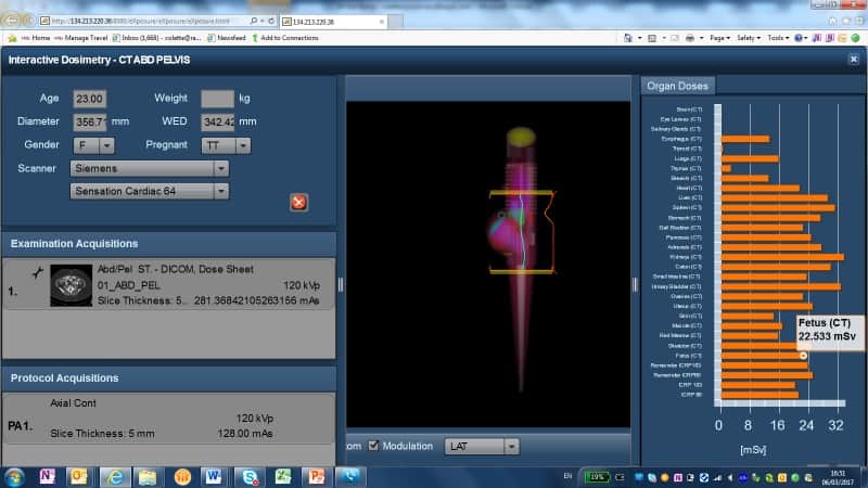
Radiation dose directives, dose management software, etc, etc – how can a busy radiologist keep up with it all? Medical physicist Virginia Tsapaki shared practical and timely information about these issues at ECR 2018 in Vienna.
The Council of the European Union (EU) established directive 2013/59/Euratom, which sets basic safety standards for protection against the dangers arising from exposure to ionizing radiation. Radiologists must be aware of some key elements, including the directive’s requirement that high-dose procedures such as CT or interventional radiology must be closely monitored, she noted. This applies to children in particular.
“Diagnostic reference levels are mandatory and require regular review and use,” said Tsapaki, from the medical physics department at Konstantopoulio General Hospital in Nea Ionia, Greece. “Clinical audits inside the radiology departments are mandatory and must be carried out in accordance with national procedures.”
Virginia Tsapaki from the medical physics department at Konstantopoulio General Hospital.
The directive clearly states any equipment used for interventional radiology and CT, as well as any new X-ray machine, must have a device or a feature informing the practitioner at the end of the procedure of relevant parameters for assessing the patient dose. The device or feature must also have the capacity to transfer this information to the record of the examination.
“At present, radiology centres in Europe, even if they are small practices, are required to collect and send a limited number of patient doses to their national legal authorities,” Tsapaki said. “In many cases, this is done manually for each X-ray room in the hospital. This can be an extremely time-consuming and complex task.”
Luckily, sophisticated software can assist in this regard, resulting in a much easier and quicker way to monitor all data included in the DICOM header of X-ray machines, or data recorded in the PACS of the hospital.
Dose management software
The users of dose management software can benchmark radiation dose levels of the hospital against national and international diagnostic reference levels. They can generate and export dose information to the examination record, explained Tsapaki, who is also president of the Hellenic Association of Medical Physicists. In the case of an outlier, an alert can be generated and sent via email or a text to the medical physicist or the person in charge.
Weekly CT scanner workload. (Courtesy: Virginia Tsapaki)
“It is very important that they are multimodality and multivendor systems and can be connected to most of the X-ray machines,” she said.
A dose management system can facilitate the evaluation of general practice and workflow of the department.
“It can reveal the habits of operators, so that corrective actions are made,” Tsapaki added. “They [systems] can help in detailed analysis of patient data for optimization of safety, quality, training, and practice of each department. The analysis of radiation dose data can be a cumbersome process that requires manual entry of thousands or even millions of values, with significant outflow of resources and the risk of typing errors.”
Estimation of foetal and organ radiation dose. (Courtesy: Virginia Tsapaki)
These systems are not cheap, and the cost usually increases with the number of X-ray devices or exams performed. However, manufacturers are making strides with this software, and, consequently, costs should fall in the future. Furthermore, dose management systems do more than collect data: They are patient management tools.
“I have evaluated a number of these systems in my hospital,” she said. “The software can easily provide end users with the time periods the X-ray machines are not in use. This helps a lot in order to schedule routine quality control and other routine tasks. Errors can be identified in protocol decisions that can be discussed with the radiographers, and in this way we could make corrective actions.”
In the future, Tsapaki anticipates that radiation skin-dose mapping specially for interventional fluoroscopy or CT procedures will reach the market.
“This will be one additional item very helpful toward personalized patient dosimetry,” she said.
Last December I was sitting in the departure lounge at Blagnac Airport in France, waiting for my flight back home to the UK. I had been at the Airbus Leadership University for the concluding part of a course, the last of several trips I made to Toulouse in 2017. Looking back over the last 30 years of my career, from starting my PhD to my current role in the Defence and Space division of Airbus, I began to think about how I progressed to my current role. Was it chance, being in the right place at the right time; was it my own making; or was it the influence of colleagues and managers? I came to the conclusion that it was a combination of all of the above, together with a carpe diem attitude in an evolving business environment that brought me here.
Having intended to study chemistry at university, I was fortunate that the broad natural-sciences course at the University of Cambridge in the UK gave me the chance to decide that chemistry was not for me after one year. So I read physics for the rest of my degree. And having been interested in astronomy since childhood, I took up some astrophysics and cosmology options in my final year, including a short dissertation on pulsar magnetospheres.
At this point I knew that I wanted to deepen my knowledge in an area of physics, but my third-year work had made me feel that I wanted to study something more tangible than stars. Inspired by some excellent solid-state physics teaching in my third year, I therefore decided to apply for a PhD in semiconductor physics at Cambridge. One of the attractions was the prospect of working in the group led by physicist Michael Pepper – known for his work on semiconductor nanostructures – and another was that the PhD was partly sponsored by the General Electric Company (GEC) Hirst Research Centre, thereby keeping open the possibilities of staying in academic research or moving into industry.
I enjoyed my research into thermoelectric transport in two-dimensional electron gases at low temperature, but by the end of my PhD, I decided to take up a research role at GEC, in its Long Range Research Lab. For most of my first three years, I was mainly based at the Cavendish Laboratory because I was working on a project based on new quantum-electronic devices, in which both the university and GEC were taking part. At this stage, I was directly using my knowledge of physics and mathematics every day – whether this was designing semiconductor devices, solving electron-transport equations or measuring the microwave performance of devices.
However, the head of GEC, Lord Arnold Weinstock, had decided he wasn’t getting enough return on his investment in a central research facility and the Hirst Research Centre gradually shrank, ending up as a division of GEC-Marconi Materials Technology before disappearing completely by the 1990s. By now I had started spending half my time working for a department that designed and manufactured quartz oscillators, surface acoustic wave (SAW) filters and thick/thin film hybrids. My first work in this group was understanding the theory behind SAW filters, and converting some SAW design-software to work in a new computing environment.
Moving forward
I quite enjoyed getting back to using Green’s functions for solving the electrostatic problem and the various tricks for getting the software to run fast enough on the mainframe computer – a job that would take three or four hours, compared with 3–4 seconds on a desktop PC today. The other half of my time was spent in the microwave group. This included some interesting work on modelling the propagation of microwaves through ferrites, and also a taste of project management, on the repair and provision of spares for the radiofrequency communications system for the Phoenix unmanned air vehicle.
I was directly using my knowledge of physics and mathematics every day
Richard Syme
I then had the opportunity to either move with the quartz oscillator group to what was then Matra-Marconi Space (now Airbus), or to keep working on the microwave systems for what would eventually become part of BAE Systems or Leonardo. I decided on the former and have been associated with quartz products ever since – first as an engineer, then a project manager and now as head of the group. Our quartz products provide the frequency or timing references in satellite payloads, mostly telecommunications satellites. The space environment is challenging for quartz oscillators – the two main difficulties are withstanding mechanical shocks and in-orbit radiation. The latter requires quartz that is very pure, since it is the impurities (principally aluminium) that give rise to a change in quartz resonator frequency with radiation. At Airbus, we grow our own quartz and it is generally recognized to be the purest in the world.
I do still use my physics knowledge regularly – my semiconductor physics helped in understanding a recent problem at a supplier of transistors – but my objectives at work now are more in line with achieving financial targets, developing people, improving products and processes and ensuring delivery of products. Physicists can be found in many groups at Airbus Defence and Space, from those working on instruments for science missions such as Solar Orbiter, BepiColombo and the Jupiter Icy Moons Explorer (JUICE), to those working on the latest digital signal-processing technology and algorithms.
One of the great things about working at Airbus is the variety of career opportunities that are available, and the training and support that exists to help you. As I mentioned earlier, I’ve been to Toulouse several times this year, to meet Airbus Defence and Space employees from all over Europe, as well as colleagues from the company’s other divisions (commercial aircraft and helicopters) – collaborative work being vital to innovate and improve for the future. This range of opportunities, and the pride in helping to produce some of the world’s best satellite products, are two of the main factors that have kept me at Airbus and given me an enjoyable and satisfying career. Airbus will always have vacancies for physicists, new graduates or those further into their careers, so I hope I have whetted your appetite to find out more about Airbus.
NASA has successfully launched a dedicated exoplanet probe that will aim to discover thousands of planets outside our solar system. Launched yesterday at 18:51 local time from Cape Canaveral Air Force Station in Florida via a SpaceX Falcon 9 rocket, the $337m Transiting Exoplanet Survey Satellite (TESS) will spend about two years surveying 200 000 of the brightest stars to search for planets.
First conceived in 2006, the mission was selected in 2013 as an astrophysics mission in NASA’s “Explorers Program”. TESS, which is 3.9 m long and 1.5 m high with a mass of 350 kg, will feature four identical 16.8 megapixel CCD cameras that each have seven stacked mirrors that help focus the light from distance stars.
The targets TESS finds are going to be fantastic subjects for research for decades to come
Stephen Rinehart, TESS project scientist
It will detect exoplanets via the transiting method, which involves looking for dips in the visible light of from a star as a planet crosses in front of it along our line of sight. By looking at how much light an object blocks, astronomers can get information about the planet’s size and by studying how long it takes a planet to orbit its star, it is possible to determine the shape of the planet’s orbit and how long it takes the planet to circle its sun.
‘A new era’
TESS’s main goal will be to detect nearby small planets that have bright host stars in the solar system so that detailed characterizations of the planets and their atmospheres can then be carried out. This will be mostly performed on existing ground-based instruments as well as with the James Webb Space Telescope when it launches in 2020.
TESS will carry on the work carried out by NASA’s Kepler mission and K2 craft, which together have discovered around 2300 and 300 confirmed exoplanets, respectively, with thousands more waiting for confirmation. While Kepler could spot planets around 300,000 light-years from Earth, it only covers 0.25% of the sky. TESS, however, will be able to see 85% of the sky searching for planets much closer to Earth, up to 300 light-years away.
“We’re going to be able study individual planets and start talking about the differences between planets,” says Stephen Rinehart, TESS project scientist at NASA’s Goddard Space Flight Center in Maryland. “The targets TESS finds are going to be fantastic subjects for research for decades to come. It’s the beginning of a new era of exoplanet research.”
A new technique that uses magnetic fields to detect underwater objects has been unveiled by physicists in the UK. The fields induce electric currents in metallic objects and the resulting magnetic echo is detected by an array of atomic magnetometers.
Detecting objects in water using electromagnetic radiation is extremely difficult because light and other radiation attenuates rapidly as it passes through water. This is not the case with sound, which is why sonar is “unrivalled in deep water” for detecting objects, according to Luca Marmugi of University College London (UCL). In shallower depths, however, the echo from the seabed can blind sonar to an object.
An alternative to sonar is magnetic detection, which can discriminate magnetic objects from non-magnetic ones. Existing schemes, says Marmugi, are passive – simply looking for any magnetic fields created by an object. “There is an obvious [military] countermeasure,” explains Marmugi. “All the steelwork composing the hull of a ship or submarine can be demagnetized and you can design engines to limit or if possible cancel all the magnetic signature.”
Secondary fields
One way forward is magnetic induction tomography, which was originally developed for industrial monitoring. This uses an oscillating “primary” magnetic field to induce electric currents in target objects that, in turn, produce “secondary” magnetic fields. By detecting these secondary fields one can, in principle, characterize any object that is an electrical conductor – as long as the object, sensors and primary source sufficiently close to one another.
“There are no countermeasures, unless you want to build a submarine completely out of something like plastic, which I don’t think is feasible,” says Marmugi.
In practice, however, deploying magnetic induction tomography in water involves overcoming severe technical hurdles, says Marmugi. Classical coil sensors are not sensitive enough to measure very weak secondary fields, so unfeasibly strong primary fields would be required.
Now, Marmugi and colleagues at UCL have created an array of four radio-frequency atomic magnetometers that can be placed under or over a container of water (see video). These magnetometers work by measuring the precession of atomic spins in a room-temperature vapour, with the precise nature of the precession being very sensitive to the presence of external magnetic fields.
Precession triggering
The primary field triggers the precession of spins in the magnetometers. If no secondary fields are excited in response to this primary field, the spins in all four magnetometers precess with the same amplitude and phase. However, any magnetic fields induced in a target will affect the precession in different magnetometers in different ways. Therefore, by monitoring the amplitude and phase in the four sensors, the researchers could detect the presence of a conductive object in the water and also determine the object’s position relative to each sensor.
The researchers demonstrated 100% success in detecting, and 91% success in locating, an aluminium plate in a beaker of salt water placed 120 mm beneath their sensor array. Salt water poses additional challenges because of its higher conductivity than fresh water.
At the 10 kHz primary-field frequency used, the wavelength of the primary signal is much longer than the range of the signal (the penetration distance). This near-field configuration had several advantages: little energy was projected deeper into the water, greatly reducing both the power consumption and the echo from deeper objects. Furthermore, the secondary field strength gives a clear indication of an object’s depth.
The researchers are now working towards testing the measurement protocol in open water. “You can achieve [near-field] penetration distances of kilometres in water if you drop the oscillation frequency to a few hundreds or tens of Hertz,” explains Marmugi. Such a system could potentially be battery powered, he says.
Better than a metal detector?
Atomic physicist Michael Romalis of Princeton University in the US, whose group has developed some of the most sensitive magnetometers ever produced, describes the research as “a fine demonstration” although he notes that the sensitivities reported are well below the best achieved with traditional coil detectors. “An old-fashioned metal detector works by just using an inductive coil for pickup. My question is ‘Is it really better than an old-fashioned metal detector?’ and it’s not obvious to me that it would be.”
Arne Wickenbrock of the University of Mainz is more optimistic: “Vapour cell magnetometers are hugely sensitive over a huge frequency range over which you cannot really build very sensitive coils,” he says, “You can also tune the frequency very easily over a broad range, which is very difficult for coils…There’s a considerable literature on eddy current detection with vapour cells but this is, I believe, the first time anybody’s used an array and detected something under water.”
There is no one right or wrong way to grow a company. Every start-up’s journey will have unique twists and turns, and although venture capital (VC) gets a lot of attention as a means of helping entrepreneurs obtain outside funds, it is hardly the only game in town. In fact, in most situations, VCs are not the optimal funding source for early-stage companies commercializing novel physical science innovations – and I say that even though I am a VC investor at a firm that supports companies doing just that. The numbers back me up: according to the crowdfunding platform Fundable, fewer than 1 in 100 start-ups are funded by angel investors and about 1 in 2000 (0.05%) are funded by VCs.
But if VC (probably) isn’t going to help your company grow, what will? Broadly speaking, external funding sources fall into four groups: grants, strategic partnerships, equity investment and debt. This list omits profits, which is perhaps the best funding source of all: when your business’s growth can be supported organically by reinvesting the profits you make from selling your product or service at a positive margin, you don’t need to bother with external entities. However, many start-ups simply cannot grow completely organically, or they want to grow faster than organic growth alone allows, at least at the outset. Therefore, external funds are often required to push a technology out of the lab.
Each external funding option has advantages and disadvantages, as well as a time and place, in the commercial journey of an advanced materials start-up. Let’s explore these in more detail, in an order that roughly aligns with how companies pass through commercial stages.
A grant to get started
Grants are often the funding source of choice to take a great idea or lab result and turn it into a bona fide start-up company. To keep things simple, when I refer to “grants”, I am also lumping in other non-equity, non-strategic-partnership funding sources. These include university business plan competitions such as the Rice Business Plan competition at Rice University in the US (the world’s richest and largest student start-up competition) and grand challenge-type programmes like the Carbon XPRIZE – a $20m global competition sponsored by NRG COSIA to mitigate or reduce CO2 emissions. Many grant programmes have a geographic component, so depending on where you are, you might want to consider applying for Horizon 2020 (EU), SBIR/STTR (US), ARPA-E (energy-related innovations in the US), or SDTC (Canada) funding if you want to commercialize a physics-based, hard tech innovation – and this is by no means an exhaustive list.
Just as in academia, grants for start-ups are competitive, and the granting body may restrict how you can use the funds.
Early in a company’s gestation, grants are a great way to bring in enough money to advance an idea into a prototype product, validate a market hypothesis, or perform additional technical development. Not only are they typically designed for early-stage and high-risk, high-reward propositions, they also don’t require you to give up any ownership or control in your company. Typically, the intellectual property – patents, trade secrets or process knowhow — developed with the support of a grant remains the company’s sole property.
Another advantage of grant funding is that companies become more valuable the closer they get to commercialization and reduced technical risk. Thus, the longer you can wait to raise outside capital, the more favourable the terms of that capital will be for you and your founding team. Hence, grants represent a good way to increase a company’s value in the eyes of a potential investor or acquirer.
The downside of grants is that, just as in academia, grants for start-ups are competitive, and the granting body may restrict how you can use the funds. Oftentimes, expenses such as marketing activities, patent legal costs and capital expenditures cannot be funded by a grant. Another word of caution is that grants are often not directly aligned with the vision, mission or strategy of a start-up. Their influence can be defocusing for a founding team, and the monetary support they offer must be weighed against the time and effort required to apply for them and comply with their terms. VC investors often avoid start-ups with an “SBIR shop” mentality as it can be hard to change the company culture into a high-growth, product-focused business.
A final challenge is that some grant programmes require the company or other investors to put up matching funding. In some circumstances, however, this can be a good way to use a small amount of outside equity capital to bring in a larger amount of money. From an investor’s point of view, this is a form of free leverage: it means that our investment buys more for our money than a traditional venture round of funding.
Howdy, partner
Start-ups are typically good at developing novel out-of-the-box solutions and nimbly pivoting and refining their approach. However, scaling up manufacturing, creating a channel to the market and/or developing the requisite trust in your (currently) no-name brand are often not a start-up’s strong suit(s). No one wants to reinvent the wheel, though, so at this stage, smartly crafted win-win partnership agreements can really help accelerate product development and market launch. Furthermore, a collaboration with a large, established company in your target market or supply chain can help validate the market’s interest in what you’re developing. For physics-based entrepreneurs, capital efficiency is the name of the game: most investors don’t have the appetite or knowledge to play in this space, so utilizing strategic money is a great path to a successful venture.
We almost always encourage start-ups to engage with strategic partners from an early stage.
Strategic partnerships can take various forms, and the devil is always in the details. However, two of the more popular strategic partnership funding models for a physical science start-up and a large company (“BigCo”) are non-recurring engineering (NRE) funding and joint development agreements (JDAs). While the nomenclature may vary, NRE typically refers to a one-time payment or a series of milestone-tied payments from BigCo to start-up that help the latter design, develop and test a new or improved product. JDAs, on the other hand, usually involve BigCo paying a start-up to develop a tailored solution that fits BigCo’s specifications and ties into a particular market; common design elements where each company pays their own expenses; and innovations that fall outside of the defined scope of the JDA, but which the start-up created while developing a solution on behalf of BigCo.
Here is an example. Let’s suppose a large steel producer signs a JDA with a thermoelectric start-up on a project to recapture and utilize waste heat from their industrial processes. During the JDA, the start-up develops a manufacturing improvement that reduces the cost of producing its industrial waste heat recovery modules by 60%. However, this improvement also applies to the combined heat and power systems that the start-up is developing for a residential market. Typically, this improvement IP, as it falls outside the scope of the JDA, is solely owned by the start-up. Hence, innovations that result from JDA funding often have important spillover effects for the start-up company’s technology platform as a whole.
The next question, of course, is how to find a suitable partner. Even if you have identified a BigCo that would benefit from partnering with you, locating the right person to speak to within their 10,000+ employee organization can be surprisingly difficult. This is an area where VC firms like Pangaea can be helpful. Our limited partners (that is, the investors in our funds) include many of the world’s leading material, chemical, industrial and electronics companies, and because we’ve been investing in advanced materials companies for over 15 years, we have developed a good network. Based on this experience, we almost always encourage start-ups to engage with strategic partners from an early stage. Assuming the agreements can be crafted in a mutually beneficial way, we believe the myriad benefits (including de-risking product development, obtaining market validation, help with creating a channel to market, identifying a potential future acquirer and, of course, the cash) outweigh potential downsides such as giving up a slice of the pie or scaring off competing strategic partners.
A stake in the game
Matthew Cohen, director of technology at Pangaea Ventures. (Courtesy: Pangaea Ventures)
The equity investor mix includes high-net-worth individuals (typically referred to as “angel investors”); “angel groups” where several such individuals participate in deals together; “family offices” where managers invest an ultra-wealthy family’s money; venture capital and private equity firms. It’s hard to generalize about why these various entities would invest or pass on a start-up, but typically, equity investors want to “add fuel to the fire” to help a start-up build its operations and thus create shareholder value. This means that, all else being equal, this group of investors will eschew “science projects” where money is earmarked for fundamental R&D work in favour of start-ups where a capital infusion will enable rapid commercial expansion.
Most VCs are looking for a plausible path to obtaining 10 times their initial investment within three to seven years. If that sounds like a tall order, that’s because it is: most investments fall well short. However, if an entrepreneur cannot convince a VC that the addressable market is large enough; the “pain point” for consumers is acute enough; the team is strong enough; and a potential acquirer will pay a high enough price – well, we’re probably going to pass. Most business cases do not fit these stringent requirements, but this certainly does not mean that they should be abandoned. It just means that VCs aren’t the right choice for funding them (at least not right then).
Raising a round of venture capital speeds up the clock for a start-up. Venture rounds typically last one to two years, and if key milestones are not achieved within that time frame, it will be tough for that start-up to raise additional funds in a successive round. Venture money can solve some problems, such as shortages of working capital or funding for expanding a firm’s capacity, but it often cannot break down fundamental technical or commercial barriers – at least, not during the time frame of a funding round.
On top of this, the rate at which firms burn through cash typically ramps up after they get VC funding. This makes it more difficult for a start-up to reposition and pursue a different path or adjacent opportunity. In general, a round of VC funding means making a bet on a specific market opportunity. There may be pivots along the way, but getting the market opportunity completely wrong is usually a death sentence. For that reason, VC funding should come in when the start-up is ready to make a good, educated guess about the market, rather than just throwing things at the wall and seeing what sticks. This is especially true for physics-based innovations. For example, a start-up company in this sector might develop a new semiconductor manufacturing process that can be used for silicon-based anodes in lithium-ion batteries, solar cells, thermoelectrics and non-volatile memory – a classic “platform” innovation. However, if they try to go after all of these opportunities simultaneously, it’s unlikely they’ll succeed with any of them. VCs want to see concrete progress on solving a major pain point in a large market, not just potential.
Venture money can solve some problems, but it often cannot break down fundamental technical or commercial barriers.
A final item to note is that when a start-up gets VC funding, its corporate governance and oversight can change almost overnight. Typically, a new board of directors is formed or an existing one significantly changed. This board will play a range of roles, including de facto “boss”. If the board believes things are not going well, or the CEO or key team members lack the skills necessary to increase shareholder value, it is the board’s fiduciary responsibility to supplement or even change the team. Even though the chances of a founder being fired from the start-up he or she founded are low, the mere possibility can be a very tough pill for an entrepreneur to swallow.
Indebted
The last source of funding for a start-up company is debt. Usually, this is more appropriate for later-stage companies with sizable balance sheets, revenue and purchase orders. While it may be possible for a pre-revenue start-up to take on debt, it’s a risky proposition. Terms around interest rates, payback periods, and penalties for missing repayment deadlines vary widely, but the last of these could include losing control of your company. Furthermore, debt holders are almost always senior to all other stakeholders and will get paid first if the company is liquidated or acquired. Some company-friendly, economic development debt programmes are certainly worth considering at almost any stage in a start-up’s life-cycle, but until a company can make good predictions about revenue amounts and timing, it’s tough to make traditional debt funding work.
The bottom line
Grants, partnerships, equity and debt are all valid options for funding start-ups. When considering which route to follow, it is worth remembering that venture capital and private equity are only appropriate for very specific subsets of early stage corporate growth. As such, VC won’t be right for most companies. However, for advanced materials start-ups that do fit the mould, we encourage you to consider getting in touch. Even if Pangaea declines to fund your venture – and that’s what we do most of the time – we always strive to assist. If we can provide feedback, introduce you to a potential partner, or even just stay on each other’s radar screens as you make commercial progress, we’re always happy to connect as you progress your innovations from the lab bench all the way through to global deployment.
“When land-clearing extent reached 40% in out models, international standards for safe drinking water were exceeded nearly 40% of the time, even if best practices for logging were followed,” said Amelia Wenger of the University of Queensland, Australia.
Wenger and colleagues believe that the logging’s impacts will compromise the integrity of the land for future agricultural uses, interrupt access to clean drinking water and degrade important downstream ecosystems, according to their press release.
Commercial logging accounts for about 18% of government revenue in the Solomon Islands and at least 60% of exports.
The Kolombangara Island Biodiversity Conservation Association is leading efforts to create a national park that will safeguard forests above 400 m with cultural and ecological significance.
“Saving tropical forests worldwide depends on tighter regulation of national laws and policies, as well as local buy-in for forest management,” said Stacy Jupiter of the Wildlife Conservation Society (WCS). “This study nicely illustrates why we need to take action now to protect the world’s remaining intact forest landscapes in order to preserve their biodiversity and important ecosystem services for people.”
Spring has just about sprung here in the UK, as the bluebells and daffodils are emerging after a long gruelling winter. In Physics World April podcast, Andrew Glester embraces the botanical theme by looking at a selection of technological innovations inspired by plants.
First up, Glester speaks with Claudia Zeiger about the idea of cleaning up oil spills using lotus leaves and a type of aquatic fern called Salvinia. Zeiger’s team at Karlsruhe Institute of Technology is interested in how these hairy-leaved species can selectively soak up oil particles while repelling water. It’s a property that could inspire more efficient clean-up operations than current approaches.
Later in the episode Glester catches up with Amirkhosro Kazemi from the department of ocean and mechanical engineering at Florida Atlantic University. Kazemi’s studies the physical properties of mangroves – common in tropical and subtropical regions – which provide a natural buffer to flood waters as well as the more routine coastal erosion. Gaining a better understanding of how these shoreline trees can dissipate water and its kinetic energy could inform the design of innovative coastal defence structures.
To find out about more nature-inspired research, check out the April issue of Physics World, a special edition on the physics of plants.
The so-called phase-separated state in perovskite nickelate materials might be put to good use in nanoscale devices such as switches or memristors. In contrast to some other technologies that exploit these materials, such devices would operate electronically rather than through redox processes or the movement of ions, and could thus be much faster.
Perovskite rare-earth nickelates, which have the formula RNiO3 are correlated oxides that undergo a metal-insulator transition during which their resistivity changes dramatically. This transition occurs at a temperature that depends on the ionic radius of the rare-earth, R. Although researchers are still unsure as to where this transition originates, it can be exploited in a variety of applications, including resistive switching and even neuromorphic computing.
Resistance maps
To date, this transition was mainly studied using macroscopic techniques. A team led by Manuel Bibes of the CNRS/Thales/Université Paris-Sud in France has now succeeded in directly imaging the local resistance of a neodymium nickelate thin film as it undergoes this transition using a scanning probe technique called conductive atomic force microscopy (AFM). The resistance maps obtained using this technique show that metallic domains between 100 and 300 nm in size nucleate in the insulating state and then grow and percolate as the temperature increases.
“In NdNiO3, the metal-insulator transition is very sharp, with the resistance dropping by a factor of 1000 or more,” explains Bibes. “What is more, the transition does not occur at the same temperature when measured upon cooling or upon warming – that is, it is hysteretic. In these types of so-called first-order transitions, the material does not continuously transform from one phase to the other, but co-exists in both phases. This is what we call phase separation.”
Pixel by pixel
Bibes and colleagues have directly observed this phase separation. “As with conventional AFM, we use a nanosized tip and scan the film surface to collect local information pixel by pixel and build up an image,” says Bibes. “The difference in our work is that we use a conductive tip (made of doped diamond) and the collected information is the local resistance. We thus construct images of the local resistance, pixel by pixel.”
At each pixel, the researchers measure the series resistance between the intrinsic resistance of the tip itself, the series resistance of the film and the contact resistance between the tip and film. “Here the total resistance is dominated by the contact resistance, which strongly depends on the metallic or insulating nature of the region in contact with the tip,” Bibes tells nanotechweb.org. “This is how we can image insulating or metallic regions.”
Faster switches
The phase-separated state might be harnessed in nanoscale devices behaving as switches or memristors, he adds. And in contrast to some other technologies, these could operate through a purely electronic mechanism rather than through redox processes or the movement of ions, and could thus be much faster.
The team, which includes researchers from ICMAB-CSIC in Barcelona, Spain, and Helmholtz-Zentrum Berlin für Materialien und Energie in Germany, says that it will now be looking into the phase-separated state in nanoscale devices made from NdNiO3. “We will also be imaging the dynamics of the resistance switching effect,” says Bibes.