The thermal expansion of graphene and several other 2D materials has been measured at a spatial resolution of just 2 nm. Robert Klie and colleagues at the University of Illinois, Chicago used scanning transmission electron microscopy (STEM) to explore the thermal properties of the technologically-significant materials. Their work could play a key role in the development of electronic components including solar panels and transistors.
Most materials expand when heated, but the rate of expansion can vary wildly between different substances – something that has important implications for the design of devices made from several materials. The change in volume is described by a material’s thermal expansion coefficient. This quantity is hard to measure for tiny samples because the measuring system itself can heat or cool the sample. This makes it very difficult to obtain an accurate measurement of the sample’s temperature.
Collective oscillations
Klie’s team realized that the temperature of a tiny sample can be determined by using STEM to fire electrons through it. As the electrons move though the material, they lose kinetic energy by creating plasmons, which Klie describes as “collective oscillations of electrons in a material”. The wavelengths, and therefore the energies, of the plasmons are determined by the size of the sample and its temperature. As a result, the amount of energy lost by electrons to plasmons is related to the temperature of the sample.
By scanning the electron beam across the sample, the team mapped changes in the plasmon energies. This provides a measure of the local temperature and ultimately the thermal expansion coefficient of the material.
Klie’s team looked at samples of transition metal dichalcogenides (TMDs), which are 2D semiconductors with unusual electrical properties. They also studied graphene – an atomically-thin sheet of carbon, which unusually, contracts when heated.
Within the temperature range 100-450 ⁰C, they found that the thermal expansion coefficients for both materials varied dramatically when different numbers of atom-thick layers were used in the sample. For TMDs, a single atomic layer expanded by a factor 45 times larger than for four layers, while the contraction of a single graphene layer was 30 times greater.
Mysterious effect
The striking result suggests that monolayers respond strongly to temperature changes when they are less inhibited by bonds to other layers. However, these interactions are known to be fairly weak – leaving a mystery that Klie hopes to investigate in further experiments.
The Arecibo Observatory in Puerto Rico has been saved following an agreement signed by a consortium led by the University of Central Florida (UCF) in Orlando. The announcement was made on 22 February by the National Science Foundation (NSF), which has been looking for an alternative sponsor for the iconic, 305 m-diameter radio telescope since 2006.
The NSF currently spends around $8m a year to keep Arecibo operating. The final impetus for the NSF to find new funding sources came in September 2017 when the telescope was damaged by Hurricane Maria, which caused devastation throughout the island and seemed to sound the death knell for the observatory. Arecibo’s mains electricity was restored in December and operations have since resumed at reduced capacity, while visitors have begun slowly returning to the observatory, which is a tourist attraction on the island.
We are very excited about this new collaboration. I believe together we can do great things and continue to push the boundaries of science
Francisco Córdova, director of Arecibo
The UCF-led consortium, known as the Arecibo Observatory Management Team, includes the Metropolitan University in San Juan, Puerto Rico, and Yang Enterprises in Oviedo, Florida, a company that operates and maintains facilities for both NASA and the US Air Force. Carlos Padin, chancellor of Metropolitan University, says the partnership will “expand the opportunities for research as well as formal and informal STEM education in Puerto Rico”, while Tyng-Lin Yang, vice-president at Yang Enterprises, says the deal would introduce “new technologies and cutting-edge tools” to modernise Arecibo’s operations.
A special place
Although the telescope’s main uses are focused on radio astronomy, space weather and atmospheric science, it is also renowned for its planetary radar facility, which NASA uses for near-Earth asteroid tracking and the characterisation of planetary surfaces. In return, the US space agency makes a $3.7m contribution to Arecibo’s annual budget. According to NASA’s 2018 budget estimate, its Near-Earth Object Observation programme will “continue to fund the operation of the planetary radar capabilities at Arecibo”.
Ray Lugo, the head of UCF’s Florida Space Institute, notes that the consortium hopes to cover some of its costs by making telescope time available to new users. “We want to bring other customers to the table,” he says, adding that the US Department of Defense could use Arecibo to test sensors while space mining companies may wish to target asteroid candidates using its planetary radar.
“The Arecibo Observatory is a very special place,” adds Arecibo’s director Francisco Córdova. “We are very excited about this new collaboration. I believe together we can do great things and continue to push the boundaries of science”.
Richard Taylor, the Canadian particle physicist who shared the 1990 Nobel Prize for Physics, has died at the age of 88. Taylor spent most of his professional life at Stanford University and the nearby SLAC National Accelerator Laboratory in California, where he did pioneering experiments that provided the first experimental evidence that protons and neutrons are made of quarks.
Taylor was born in 1929 in Medicine Hat, Alberta and decided to pursue physics after the atomic bomb blasts at the end of the Second World War. He described himself as “not an outstanding student”, and did not graduate from high school. However, a teacher managed to get him into the University of Alberta based on his ability to do mathematics and science.
After doing bachelor’s and master’s degrees at Alberta, Taylor went to Stanford in 1952 where he began work on a PhD that involved an experimental study of pion production. In 1958 he took a break from his dissertation and spend three years in France, helping to build the Laboratoire de l’Accélérateur Linéaire at Orsay. He then worked briefly at the Lawrence Radiation Lab in California before returning to Stanford in 1962 to work on the nascent Stanford Linear Accelerator (SLAC) and complete his PhD.
Taylor bagged his Nobel prize along with Jerome Friedman and Henry Kendall – who were both at the Massachusetts Institute of Technology. In the late 1960s and early 1970s the trio was at the forefront of an experiment at SLAC that involved firing high-energy electrons at protons and neutrons. They found that electrons underwent much more “deep inelastic scattering” than was expected. This involved the electrons giving up large amounts of energy to the proton or neutron and undergoing large deflections from their original trajectories.
This unexpected observation was the first experimental evidence that protons and neutrons were made of three particles called quarks – a concept that was introduced in 1964 by Murray Gell-Mann and George Zweig.
Industrial fishing covers more than 55% of the ocean’s surface – over four times the area covered by agriculture. That’s according to a team who used ship tracking technology, satellite feeds and machine learning to create a high-resolution dataset.
The analysis looked at 70,000 vessels, including more than three-quarters of the world’s industrial fishing ships larger than 36 m. The dataset is freely available.
“By publishing the data and analysis, we aim to increase transparency in the commercial fishing industry and improve opportunities for sustainable management,” said David Kroodsma of Global Fishing Watch, a collaboration between Google, Skytruth and Oceana.
The dataset provides greater detail than previously possible about fishing activity on the high seas, beyond national jurisdictions, according to a press release from Global Fishing Watch. While most nations appear to fish predominantly within their own exclusive economic zones, China, Spain, Taiwan, Japan and South Korea account for 85% of observed fishing on the high seas.
“This dataset provides such high-level resolution on fishing activity that we can even see cultural patterns such as when fishers in different regions take time off,” said Juan Mayorga of the National Geographic Society’s Pristine Seas project and the University of California Santa Barbara, US. “Data of this detail gives governments, management bodies and researchers the insights they need to make transparent and well-informed decisions to regulate fishing activities and reach conservation and sustainability goals.”
The figure of 55% is likely to be an underestimate as some regions have poor satellite coverage and some exclusive economic zones have a low percentage of vessels that use automatic identification systems (AIS).
“This study reveals fishing as an industrial process in which vessels operate more like floating factories that need to operate around the clock to make money,” said Boris Worm of Dalhousie University, Canada. “On the upside, however, this dataset also shows clearly where management boundaries are in place and where they are helping to constrain fishing effort.”
The researchers used machine learning to analyse 22 billion messages broadcast from AIS from 2012–2016. These revealed the vessels’ movement patterns, enabling the team to identify more than 70,000 commercial fishing vessels, the size of their engines, the type of fishing they were conducting, and where and when they fished to the nearest hour and km.
“Only a few years ago, we didn’t have the computing power, enough satellites in orbit, or techniques to run machine learning at scale over massive datasets,” said Brian Sullivan of Google Earth Outreach. “Today we have all three, leading to dramatic advances in our ability to monitor and understand human interaction with our natural environment.”
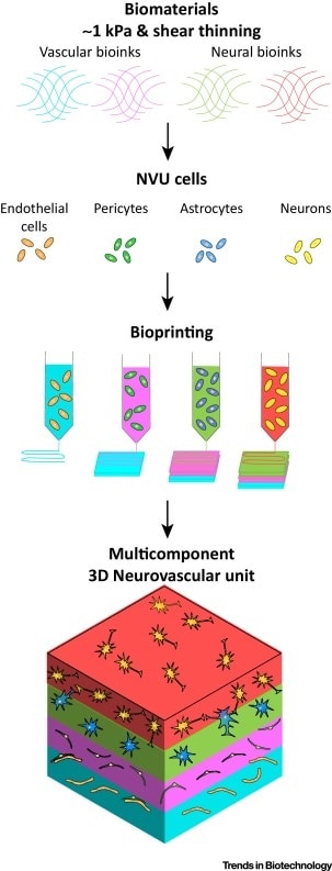
The onset of many neurodegenerative diseases, such as Alzheimer’s and stroke, is directly related to the dysfunction of the neurovascular unit (NVU). For this reason, 3D models that closely mimic the complexity of the NVU are needed to investigate what goes wrong during pathogenesis. Tissue engineering offers a plethora of advanced techniques to achieve this goal. Among them, bioprinting seems the most promising, allowing the deposition of novel biomaterials and bioinks to recreate NVU-mimicking structures.
The NVU is a brain-localized unit, composed of a vascular and a neural component. The correct cross-talk between these two components is fundamental for brain health, since it regulates transport of oxygen and nutrients to the brain, along with removal of toxic compounds, preventing neuroinflammation and neurodegeneration.
The NVU extracellular matrix (ECM) represents the medium through which neural and vascular components can interact, providing physical support and biochemical cues to embedded cells. Indeed, the ECM can provide stimuli to promote growth of new neurons and blood vessels, as well as maintenance of brain health over time. For these reasons, disruption of the NVU has been linked to the onset and progression of severe neurodegenerative diseases, such as Alzheimer’s, vascular dementia, Parkinson’s and stroke.
Modelling the neurovascular unit
To understand what goes wrong during dysfunction of the NVU, researchers need new models that can accurately replicate the complex interactions between cells and ECM components in the NVU. Although different animal models exist for this purpose, there is a need to develop human cell-based models, which can be studied in large scales, to dissect precise cellular roles in disease, and for specific human-related experiments.
In this direction, recent progress in tissue engineering has made possible the fabrication of complex structures consisting of different cell types and different materials. Bioprinting stands out among novel tissue engineering techniques, since it allows the precise deposition of cells and material in a layer-by-layer fashion to recreate organized 3D constructs. Bioprinting can be either direct, when the biological material – bioink – is deposited directly to recreate the 3D structure, or indirect, when final structures are obtained by removing additional material used as temporary mould.
NVU model
Exploiting these techniques, cells can be encapsulated in water-rich gels, also called hydrogels, which are in turn printed to form 3D structures. For example, endothelial cells can be printed in patterns that mimic the microvasculature of the vascular unit, while neurons and glia can be deposited as interconnected parts to fabricate the neural component. Moreover, these two components can be interfaced by simply printing them as two consecutive layers to mimic the neuro-vascular interactions.
Due to the role played by ECM, researchers can also choose to tune the mechanical and biochemical cues of the NVU models by choosing different bioinks. For example, stiffer or softer hydrogels can be printed according to the stiffness required, while inner porosity and local chemistry of the matrix can be dictated by printing natural or synthetic materials with inherent characteristics.
Therefore, the specific choice of bioinks can lead to fabrication of high-quality and complex NVU models. Moreover, the possibility to finely design these constructs and produce them in large scale makes 3D bioprinted NVU models a valid research tool for the future study of neurodegenerative diseases, moving the field a step forward.
With an icy wind whipping into southern Sweden from Siberia, the site on which the European Spallation Source is being built was not the most clement place when Physics World visited earlier this week.
My colleague Margaret Harris and I had travelled to Lund to catch up with the latest progress on the ESS, which – when complete in 2025 – will be the most advanced facility for neutron scattering in the world. It will outstrip the likes of the Spallation Neutron Source in the US, ISIS in the UK and the China Spallation Neutron Source.
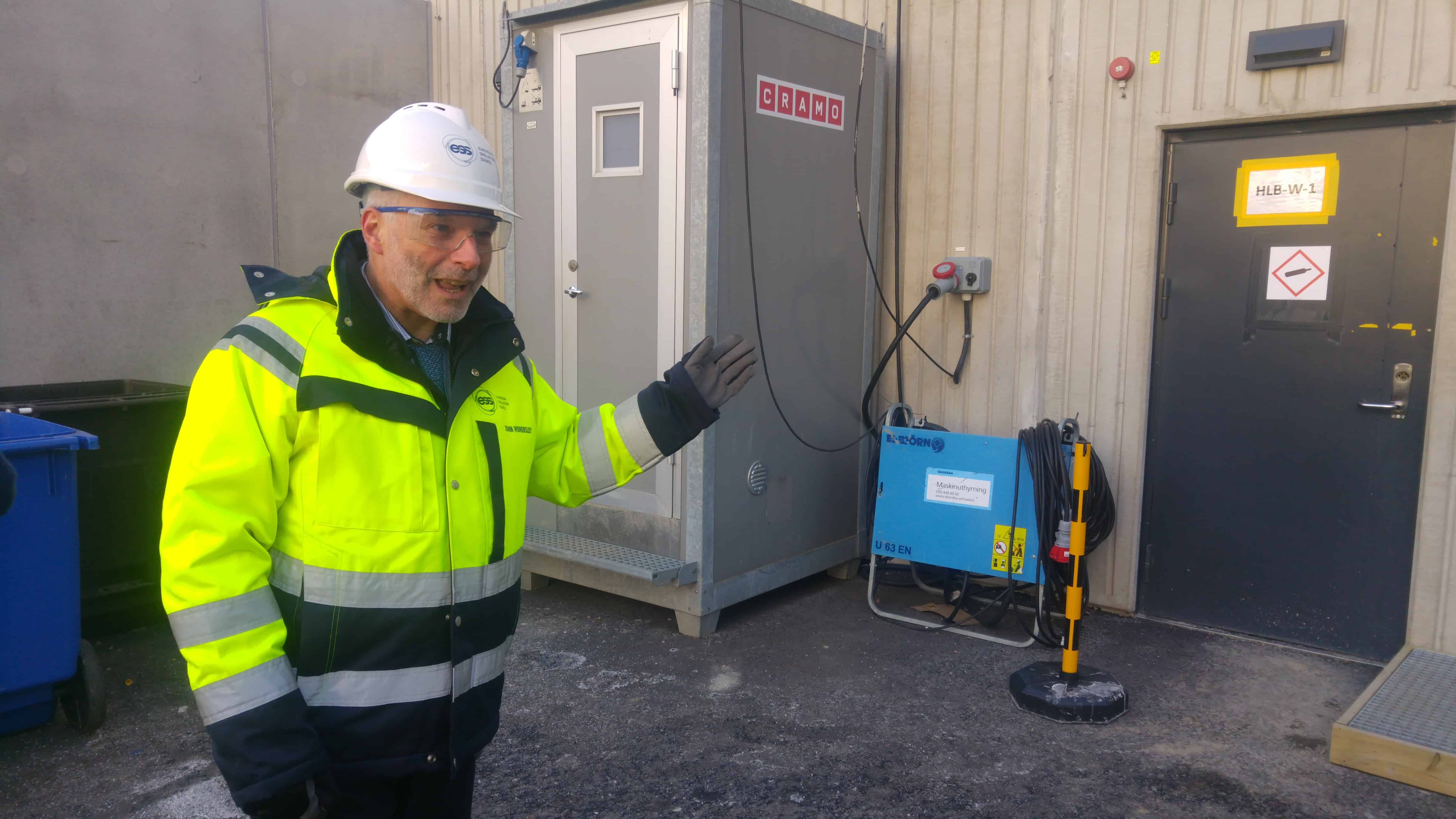
With the late-afternoon Sun casting long shadows over the freezing 65,000 m2 building site, we were accompanied on our tour by John Womersley, the British physicist who took over as director-general of the ESS in 2016.
Decked out in hi-vis jackets, safety helmets, glasses and gloves for our tour of the construction site, Womersley explained how the ESS is a consortium of 15 European nations and will cost a total of €1.84bn to build.
Work started on the project in 2014 and is now 40% complete. This year is the peak period for building activity and there are currently 500 workers on site. “So far things are going quite well,” Womersley said as he led us from the warmth of the lab’s temporary office accommodation through security turnstiles to the construction site. “We are more or less on schedule.”
Our visit to the ESS formed part of the inaugural Big Science Business Forum, which is taking place in Copenhagen this week. Most big-science facilities – be it CERN, the European Southern Observatory or the European Synchrotron Radiation Facility – are known for their cutting-edge research. But these facilities are also hotbeds of advanced technology, offering opportunities for businesses to make money and to hone their technological innovation.
The ESS is no exception, requiring everything from radio-frequency power sources, accelerator components and vacuum equipment to cryogenic kit, neutron detectors, control systems and IT resources.
Straight ahead: the 500 m-long tunnel will house a proton accelerator, but is now mostly empty. (Courtesy: Margaret Harris)
When complete, the ESS will consist of a 500 m-long linear proton accelerator with an average beam power of 5 MW, making it the world’s most powerful such device in the world. It will accelerate protons to an energy of 2 GeV before smashing them into a rotating, helium-cooled tungsten target wheel, some 2.6 m in diameter. The protons will split, or “spall”, the tungsten nuclei to yield 10 pulses of neutrons every second. The tungsten rotates to prevent it from overheating – if the protons were fired into a fixed target, it would be in danger of melting, such is the heat load of the beam.
These pulses will then be slowed down, or “moderated”, by bouncing them off the inside of a waveguide cooled by liquid hydrogen, and sent to 15 experimental stations in three experimental halls the size of seven football pitches. When the first experiments on the ESS begin in 2023, users will have seven instruments to pick from. The full programme of activity, with 22 instruments covering large-scale structure, diffraction and spectroscopy, will be ready two years later, although longer term there is capacity for 40 instruments in total.
Neutrons have several well-known advantages when it comes to probing matter. They are charge neutral, which means they penetrate deeply into samples. They have a spin of one half, allowing them to probe magnetic materials. And because they scatter off atomic nuclei, there are therefore sensitive to light elements and isotopes, such as hydrogen. X-rays, in contrast, scatter in proportion to the density of electrons in an atom, meaning they work best only with heavier atoms.
Come on in: European Spallation Source director John Womersley points to the door leading to the tunnel that will house the proton accelerator. (Courtesy: Matin Durrani)
Most of the ESS seems a bit of a mess – well, it is a building site – and it is hard for the untrained eye to get a sense of how it will finally look. Part of the reason is that the main proton accelerator is hidden five metres underground, currently accessible only via an inconspicuous dark-grey door.
As Womersley led us through and down a metal staircase, he explained that the tunnel is located underground to keep environmental conditions for the beam as stable as possible and to ensure that, should the beam veer off accidentally into the sides of the magnets that focus it, no-one will be at risk from the dangerous X-rays that would be created.
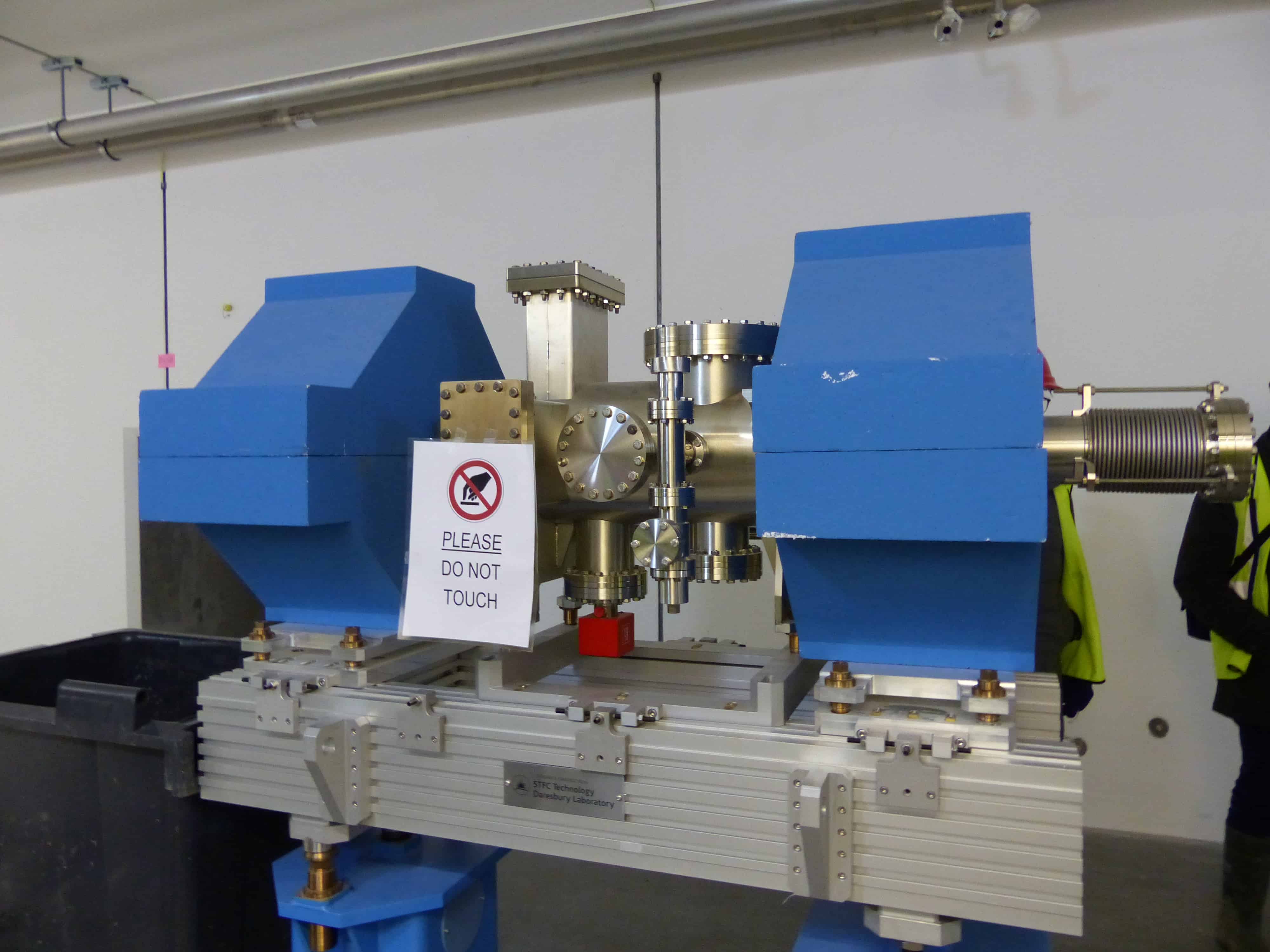
Down, down: a linear accelerator warm section from the UK’s Daresbury Laboratory in the tunnel at the European Spallation Source. (Courtesy: Matin Durrani)
With white walls and fluorescent lighting, the tunnel stretches into the distance and is largely empty. But over the next three years, it will steadily be filled with 36 metal cavities, each of which will receive radio-frequency (RF) waves sent via waveguides from five-metre-tall klystrons sitting in a large “gallery” building above ground that looks like the inside of a warehouse. The cavities will transfer power to the beam, effectively kicking the protons down the tunnel.
Scene of the action: John Womersley in the gallery building at the European Spallation Source. (Courtesy: Matin Durrani)
One novel feature of the metal cavities is that they will be cooled to cryogenic temperatures so that they superconduct and therefore transfer the RF power with almost 100% efficiency, with none absorbed by the cavity. There are already two klystrons being kitted out in the gallery, with Womersley explaining that the first prototype cryomodule is set to be tested in July. Hatches have already been built into the walls of the tunnel to allow the waveguides to pass through from the klystrons above.
Cold prospect: these towers will recycle the helium needed for the European Spallation Source. (Courtesy: Matin Durrani)
Back in the open air again, Womersley pointed out three helium cooling towers rising above the rubble. Built in Liverpool, they will eventually be used to recycle the 3.5 tonnes of helium needed for the ESS. Indeed, sustainability is the name of the game for the ESS. Although the lab will take a whopping 25 MW of power from the local electricity grid to run the accelerator, all waste heat will be connected to Lund’s heating system rather than just being vented into the atmosphere.
The heat is in fact just one benefit to the local economy of the ESS, which will eventually have 400 scientists, engineers and ancillary staff working permanently on site. Local shops, hotels and businesses will also gain from the thousands of scientists who will visit each year. And with the existing MAX-IV synchrotron barely a few hundred metres away from the ESS, there are ambitious plans to create a “Science Village Scandinavia” in the land between the two facilities.
The ESS is certainly an ambitious project, with the neutrons set to be used in everything from soft matter, chemistry and energy to magnetism, geophysics, basic physics, archaeology and heritage conservation. “Our plan is for the ESS to run 95% of the time for 200 days per year,” says Womersley, “so we need a machine that is reliable.”
Meanwhile, Denmark – the joint host with Sweden of the ESS – will be boosted by an IT and data centre in Copenhagen that will employ 60 staff. The idea is that all data generated in experiments at the ESS will be “open” once a three-year period has elapsed, which will allow anyone, in principle, to analyse results obtained at the lab.
As we headed back to the Danish capital over the Øresund bridge with the red Sun setting in the west, I was left with a warm, fuzzy feeling of Europe with its open science and open borders. Quite why Britain wants to quit the EU, when there is so much to play for in building a strong European science base, I simply cannot fathom. It was a question I was to put to Womersley at the BSBF meeting back in Copenhagen. Stay tuned for his response.
The optoelectronic properties of topological insulators have many attractions, including a robustness to defects, imperfections and sharp corners. This robustness inspired a group of scientists to design and demonstrate the feasibility of a topological insulator laser. The resulting laser is reported to preserve single-mode lasing even at very high gains.
While the first discovered topological insulators were electronic, nowadays scientists have developed them in many other physical systems, including photonic, mechanical, acoustic and cold atoms. In all these systems, topological insulators are defined by the transport properties, in that the bulk is insulating but the surface or edge states are conducting.
In topological insulator lasers, light can move around the cavity of any shape without scattering or disorder. It also propagates in a unidirectional fashion, unaffected by the shape of the edges. This robustness to defects, fabrication imperfections and sharp edges gives topologically protected states an advantage over conventional cavity modes for lasing.
The theory
Efficient lasers that are more immune to operational disorder and defects may be possible by exploiting topological properties, as a group of scientists from Israel, Singapore and the USA, led by Mordechai Segev from Technion, Israel and Mercedeh Khajavikan and Demetrios Christodoulides from CREOL at UCF, Florida, demonstrate both theoretically and experimentally in two recently published papers.
For the theoretical analysis, the group simulated several planar arrays of active coupled ring resonators, including the Haldane toy model – a honeycomb ring of micro-resonators. An output coupler collects the light from the cavity and verifies the working conditions of the structure. In fact, the Haldane model exhibits two distinct phases: a trivial phase and a topological one, which can be controlled by tuning the coupling between the resonators. In the topological phase the edge states, existing around the conductive edges of the structure, appear and propagate around the cavity. This, however, is not the case for the trivial phase, in which the lasing mode localizes and never reaches the output coupler. Light reaching the output coupler therefore signifies that topologically protected states are lasing in the cavity.
Segev and colleagues then introduced disorder and defects into their cavities (such as a missing resonator along the edge of the cavity) and verified that the edge mode remained unaffected. However, for the trivial-phase cavity, the presence of either disorder or defects reduces its already weak external coupling.
In practice
For the experimental realization, the CREOL-Technion collaboration fabricated two 10×10 arrays of microresonators on an active platform of 30 nm thick InGaAsP quantum wells, one of them being topological and the other trivial. They interrogated the edge states by pumping the structure under various conditions and measured the light at the output coupler. Independently of the pumping structure (i.e. which micro-resonators were excited), the edge states in the topological lattice example always travelled around the structure reaching the output coupler. The trivial structure differed in that the modes localize and cannot make it to the output.
Details are available in two recently published papers covering both the theory and experiment.
Edible electronic circuits have been made by modifying a technique for transferring temporary tattoos. The process was developed by scientists in Italy, South Korea and Japan who say that the transfers are completely ingestible – and could be used to create electronic tags that could be monitored as they travel through the body. The team has also shown how the circuits can be transferred to a range of edible items including fruit and drug capsules.
Ingestible electronic devices have great potential for medical treatment and point-of-care testing. They could perform diagnostic tests or control the release of a drug, and transmit data to healthcare professionals. Such technology could also have applications in the food industry, particularly for tracking and monitoring food as it moves through the supply chain.
Bitter pills
Most devices proposed so far have used large silicon-based electronics that are costly to produce, making them unsuitable for mass produced, single-use items. “Edible or ingestible electronics is typically approached by means of common silicon chips and bulky electronics, encapsulated in an ingestible pill (an inch long, typically),” explains Mario Caironi, at the Polytechnic University of Milan, in Italy. “Such a pill has to be evacuated from the body after its function.”
Writing in Advanced Materials, Caironi and colleagues say that tattoo paper – the paper used to create the temporary tattoos loved by kids everywhere – could offer a more functional approach. They say it is ideal for edible electronics as the transfers are made from ethyl cellulose, an ingestible material commonly used in medicines and as an emulsifier in food, and can be easily printed on.
Tattoo you
Temporary tattoos consist of a thin film of ethyl cellulose – which the design is printed on – stuck to a paper sheet with water-soluble starch or dextrin. To apply the tattoo, you soak the paper in water and place it on your skin and as the starch or dextrin dissolves peel the paper away, leaving yourself ‘tattooed’.
To test their idea, Caironi and colleagues used an ink jet printer – designed for printing electronics and displays – to print electronic circuits made of silver and mixes of four different semiconducting polymers on tattoo paper. They printed a range of transistors and logic gates, and transferred them on to drug capsules, strawberries and glass microscope slides.
“The tattoo releases a half-a-micron thick cellulose layer, which is edible, with our transistors and circuits printed on top,” says Caironi. “The technique is key to our proposed approach, as it decouples the printing – which can be potentially done on small scale – from the integration with edible items, which do not require any pre-treatment.”
Variable results
The effect of the transfer process on the circuits varied with different transistors, logic gates and polymers. In some cases, the effect on functionality was small, while for others there was a marked deterioration. The researchers put these issues down to impurities introduced when the circuits were exposed to air, light and water during the transfer process. They believe that adjusting the material mixes would create more stable circuits.
A key issue with ingestible electronics is biocompatibility. The team point out that the recommended dietary allowance of silver for someone weighing 70 kg is 350 μg. A single printed transistor contains around 4 μg of silver. Two of the polymers used – poly(3-hexylthiophene) and polystyrene – are known to be biocompatible, while the other two have only recently been developed and their toxicity is unknown. The researchers conducted some basic laboratory tests, with promising results, but say that dedicated studies will be needed to determine the biocompatibility of these materials.
Edible logic
Christopher Bettinger, from Carnegie Mellon University in Pittsburgh, in the US, says of the journal article describing the tattoos: “This is a really interesting paper that explores the interface of organic electronics, printing technology, flexible devices, and ingestible electronics”. He adds, “This technology adds to the growing list of materials, techniques, and manufacturing methodologies that are dedicated to increasing the capabilities of electronic devices that can be deployed to the gastrointestinal tract through the oral route”. “The transistors described here could be used as logic elements for ingestible sensors or smart controlled release devices. What remains to be seen is how these devices can perform stably in the potentially caustic environment of the stomach and small intestine.”
Caironi says, “We took a first step, demonstrating that we can transfer printed circuits on edible items”. “We have on the one hand to go deep in the assessment of edibility of the semiconductors. On the other, we have to progress at the system level, integrating our circuits with sensors, for different applications, with edible batteries and with a suitable communication system.”
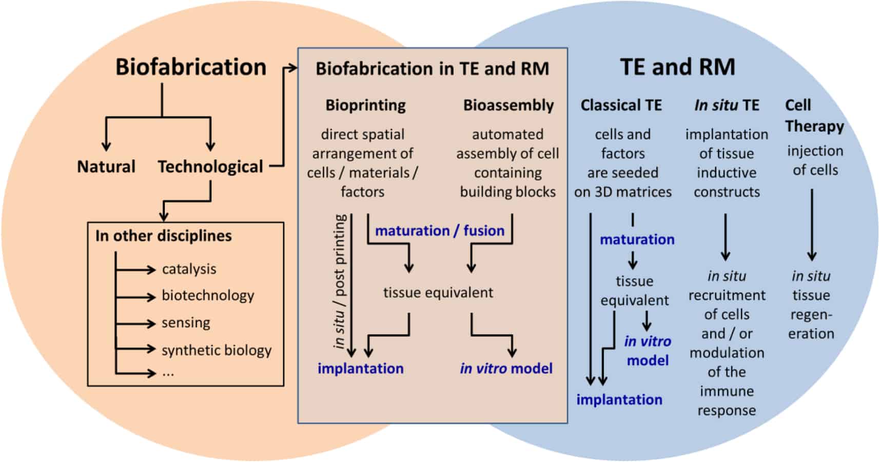
Biofabrication can mean different things to different people, particlularly as the field evolves, expands, and attracts more researchers across a variety of scientific disciplines. Custom manufacturing techniques such as 3D printing are opening the door to more effective treatments for damaged joints and organs, while biofabrication also benefits healthcare in other ways – for example, by providing tools to help drug screening and pharmaceutical development.
To help everyone navigate this rapidly evolving research landscape, representatives of the community joined forces to propose a working definition of biofabrication that highlights key areas of activity taking place today. One of the main goals of the study, originally published as a Perspective article in the journal Biofabrication, is to clarify the relationship between biofabrication and tissue engineering and regenerative medicine – two major application areas for the field.
In this context, the multicentre team defines biofabrication as: “The automated generation of biologically functional products with structural organization from living cells, bioactive molecules, biomaterials, cell aggregates such as micro-tissues, or hybrid cell-material constructs, through bioprinting or bioassembly and subsequent tissue maturation processes.”
Branches of biofabrication
The reappraisal exercise brought together biologists, chemists, materials specialists, engineers and medical experts, who took the opportunity to explore the history of their shared field. “The definition is the result of an intensive discussion and represents a consensus of many leading scientists in the field,” says Jürgen Groll, a researcher who was involved in the process and leads a group based at the University of Würzburg, Germany.
Drivers behind the rapid growth of biofabrication include advances in additive manufacturing and the use of printing technologies to position cells in 3D – a process dubbed as “cytoscribing” by Robert Klebe in 1988.
Groll and collaegues explain that biofabrication as a term was first coined in 1994 to describe natural processes such as the biomineralization of pearls. Other examples in this category include a reference to the deposition of enamel in mammalian teeth. Additional milestones include the appearance of the term “organ printing” in 2003, a phrase that has captured people’s imagination and is still used frequently today.
Two years on from Groll and colleagues’ reappraisal, biofabrication can be found describing the generation of nanostructured assemblies containing biological materials. And updating the picture further, subsets of the broader field also include uses in catalysis, sensing, synthetic biology and other technological disciplines.
Groll is keen to unravel the true potential of the technology and points out that the biofabrication is still a young and evolving field. “Within the context of tissue engineering and regenerative medicine, it’s less than 20 years old,” he explains.
Full details of the team’s work on reappraising this evolving field can be found in the journal Biofabrication.
This article is the first in a series of reports reviewing progress on high-impact research originally published in the IOP Publishing journal Biofabrication in 2016.
Urban agriculture is on trend. From restaurants that harvest their salad leaves from exterior walls, to town-centre planters where passers-by can nibble a strawberry or two, people are finding inventive ways to grow food in urban areas. Now a review indicates that exploiting waste streams – heat, light and wastewater – could lead to a new wave of ultra-efficient urban agriculture schemes.
Currently an estimated 15% of total US energy demand comes from the food system. Fertilising and heating crops, then transporting them from farm to fork, requires significant amounts of energy. Now, Eugene Mohareb from the University of Reading, UK, and colleagues have performed a literature review to provide new insights into the energy implications of scaling up urban agriculture in cities in high-income countries.
Given that more than 75% of energy use in the food system of high-income countries is estimated to occur beyond the farm gate – in transportation, packaging, processing and waste management – it’s clear that urban agriculture has the potential to cut energy use, as previous studies have indicated.
However, in some circumstances urban agriculture can increase pressure on resources and make higher energy demands. “Urban agriculture projects that rely on artificial light sources can require much greater energy inputs than otherwise, even when considering increased yields,” said Mohareb. Meanwhile, water in urban areas is likely to come from municipal water treatment plants so is generally more energy intensive to produce than, say, irrigation water from local surface water.
With this in mind, Mohareb and his colleagues stress that any increase in urban agriculture needs to consider where these additional inputs – heat, water, light and nutrients – are going to come from and how their energy impact compares to conventional farming.
But sometimes these problems can be overcome by making use of urban waste streams. “Many institutions and businesses have large centralised heating systems, often relying on natural gas as a fuel, whose waste heat and carbon dioxide is simply exhausted,” said Mohareb.
Integrating urban agriculture into these locations and tapping into the rich waste stream can be a win–win situation. Already there are examples, with the likes of Evesham Vale Growers using anaerobic digesters to process all their waste, with the resulting carbon dioxide and heat fed back into the greenhouses. Meanwhile, wastewater and storm-water streams are currently underexploited, but could help relieve the pressure that urban agriculture places on municipal water and wastewater treatment plants.
Ultimately, Mohareb and his colleagues conclude that there are no “one-size-fits-all” recommendations for urban agriculture, and that each location needs to consider its local circumstances.
“Crop type, local climate, production method and scale, availability of waste resources, co-location approaches and intensity of production all need to be considered,” writes the team in Environmental Research Letters (ERL) . But without a doubt there is potential for urban agriculture to grow and play a role in making food production more energy and resource efficient.