Many years of effort were needed to develop blue light-emitting diodes and lasers, but devices based on indium gallium nitride are now set to revolutionize optoelectronics. The first blue laser, unveiled in 1995, caused much excitement in the optoelectronics industry. Shuji Nakamura describes the advances that enabled his group to end over 30 years of research and development
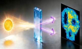
Light-emitting devices based on semiconductors have had a huge impact on modern technologies. The brightness and durability of light-emitting diodes make them ideal for displays, while semiconductor lasers have been used in everything from optical communications systems to compact disc players. But these applications have been limited by the lack of materials that can emit blue light efficiently. Full-colour displays, for example, require at least three colours, usually red, green and blue, to produce any visible colour. Such a combination is also needed to make a white light-emitting device that would be more durable and use less power than conventional bulbs or fluorescent lamps.
Many other applications would benefit from blue light-emitting devices. The shorter wavelength means that the light can be focused more sharply, which would increase the storage capacity of magneto-optical and optical disks. Digital versatile disks, which came on the market in 1996, rely on red semiconductor lasers and have a data capacity of about 4.7 Gbyte, compared with 0.65 Gbyte for compact discs. By moving to blue wavelengths, the capacity could be increased to 15 Gbyte. Blue laser diodes could also improve the performance of laser printers and undersea optical communications.
Efficient blue-emitting devices were first demonstrated by my group at Nichia Chemical Industries in Japan in 1995, after about 30 years of research by groups around the world. Such was the need for these devices that blue and green light-emitting diodes based on indium gallium nitride are already being used in a variety of applications, such as traffic lights and full-colour displays. Blue semiconductor lasers were also introduced in 1995, and today can achieve a lifetime of 10,000 hours under continuous operation at room temperature.
Light from semiconductors
A light-emitting diode (LED) essentially consists of an “active” layer of semiconducting material sandwiched between n-type and p-type semiconductors. When a voltage is applied to the junction, electrons from the n-type material move into the conduction band of the active layer, while holes from the p-type semiconductor are injected into the valence band. Light emission takes place when electrons at the bottom of the conduction band spontaneously recombine with holes in the top of the valence band.
If many more electrons and holes are injected into the active layer, a “population inversion” takes place between the conduction and valence bands. By including mirrors at both sides of the active layer to form a so-called waveguide cavity, the emitted light can be amplified and strong stimulated emission is observed at the edges of the cavity. This device is called a laser diode.
The key point is that the wavelength of the emitted light, and hence its colour, is determined by the band gap of the active layer. The wavelength is given by l = hc /E g, where h is Planck’s constant, c is the speed of light and E g is the band gap. The band gaps of compound semiconductors such as aluminium gallium arsenide and aluminium indium gallium phosphide make them suitable for fabricating efficient red and yellow light-emitting diodes, but until recently there have been no suitable materials for comparable blue light-emitting devices.
Although blue and green light-emitting diodes have been made from materials such as silicon carbide and gallium phosphide, they are not very efficient. These materials have an indirect band gap, which means that the electrons and holes have different momenta and can only recombine by scattering from lattice vibrations. In a material with a direct band gap, the electrons in the conduction band can recombine directly with holes in the valence band, making recombination much more efficient.
Although many researchers have investigated various direct-band-gap materials for blue and green light-emitting devices, it has proved extremely difficult to produce efficient and reliable devices. The most intense research has focused on II-VI materials such as zinc selenide and III-V nitrides such as gallium nitride, since these materials have a large enough band gap to emit light at blue and green wavelengths.
The advantage of II-VI compounds is that they can be deposited easily on a gallium arsenide (GaAs) substrate with a relatively low density of defects. This is because materials like zinc selenide have a similar lattice constant to GaAs. Any mismatch in lattice constant creates strain in the layers, which is generally released as misfit dislocations. In the case of red-emitting devices, aluminium gallium arsenide has almost the same lattice constant as GaAs, while aluminium indium gallium phosphide can be lattice-matched to gallium arsenide by altering its composition.
Materials based on zinc selenide have been studied intensively for use in blue- and green-emitting devices. Indeed, in 1991 Michael Haase and colleagues at 3M in the US demonstrated the first pulsed operation of green laser diodes based on II-VI materials. However, the lifetime of these laser diodes is only about 100 hours, a limitation that has prevented them from being commercialized.
These short lifetimes are thought to be due to crystal defects. Even though there are relatively few defects in II-VI materials, about 1000 cm-2, a single defect can cause others to propagate, disrupting the weak bonding in the material and causing the device to fail. This is not expected to be such a big problem in III-V nitrides because the bonding is much stronger.
Gallium nitride and other III-V nitrides also have a direct band gap that is suitable for blue light-emitting devices. The band-gap energy of aluminium gallium indium nitride varies between 6.2 and 2.0 eV, depending on the composition at room temperature. However, there is no lattice-matched substrate for the growth of gallium nitride. Sapphire is commonly used, despite a mismatch of 13.5%. Other options are silicon carbide and magnesium aluminate, which have mismatches of 3% and 9%, respectively.
Such large differences in lattice constant create misfit dislocations at the interface between the gallium nitride and the substrate. Although the number of defects can be as high as 1010 cm-2, these dislocations do not seem to reduce the efficiency of light emission and have not prevented the development of practical devices. Moreover, since these materials are bound much more strongly than the II-VI materials, devices based on gallium nitride are expected to be more reliable.
So far, only a ternary compound, indium gallium nitride, has been used as the active layer of blue and green light-emitting devices. As we shall see, the addition of indium to gallium nitride is vital for achieving strong light emission. The band gap of the material can be varied between 2.0 and 3.4 eV by altering the indium content, which corresponds to emission wavelengths between 620 and 365 nm.
Routes to blue devices
One of the main problems in the development of devices based on III-V nitrides was the lack of p-type materials. Although n-type gallium nitride is easy to produce, researchers had struggled to make p-type gallium nitride since the 1960s. The usual approach has been to dope the material with impurities such as zinc, magnesium and beryllium. These should accept electrons when positioned at gallium sites, and so generate large numbers of holes in the material. However, this approach did not produce p-type gallium nitride with good hole conductivity, and no-one understood why.
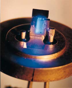
The breakthrough came in 1989, when Hiroshi Amano and colleagues at Nagoya University in Japan obtained thin films of p-type gallium nitride for the first time. They used metal organic chemical vapour deposition (MOCVD) to produce films doped with magnesium. Gases of trimethylgallium, ammonia (NH3) and bis-cyclopentadienyl magnesium were supplied to the sapphire substrate by a hydrogen carrier gas. The substrate was heated to 1000 °C, causing the precursor gases to react and form a thin film of gallium nitride on the surface. After growth, the films were irradiated with a low-energy electron beam, and the resulting film was found to be p-type, although the hole conductivity was poor.
It seems that the effect of the electron beam was to move the magnesium atoms to gallium sites. Before irradiation, the magnesium atoms cannot act as acceptors because they are not positioned at gallium sites. By moving the magnesium atoms with the electron beam, the impurities can act as acceptors and generate large numbers of holes. At the time, however, this mechanism was not fully understood and other groups were unable to produce p-type gallium nitride for another few years.
At Nichia, colleagues and I first obtained p-type gallium nitride films in 1992. Rather than treating films of magnesium-doped gallium nitride with an electron beam, we thermally annealed the layer in a nitrogen atmosphere at temperatures above 700 °C. Annealing was found to reduce the resistivity of the films from 106 W cm to just 2 W cm.
To help understand this change in resistivity, we tried two further annealing experiments. If the low-resistivity p-type films were further annealed in nitrogen at temperatures ranging between room temperature and 1000 °C, the resistivity remained almost constant at 2-8 W cm. However, if the films were annealed in ammonia at 600 °C, the resistivity increased to as much as 106 W cm.
So what causes the change in resistivity? The key seems to be the effect of atomic hydrogen, produced by the dissociation of ammonia at temperatures above 400 °C. Since dissociation occurs at the gallium nitride surface, hydrogen atoms can easily diffuse into the gallium nitride. Once inside the film, the hydrogen atoms form neutral complexes with the magnesium impurities and stop them from acting as acceptors.
This hydrogenation process is probably responsible for the surprisingly high resistivity of magnesium-doped gallium nitride films. The effect of thermally annealing the films in a nitrogen atmosphere is to remove atomic hydrogen from the neutral complexes, reactivating the magnesium acceptors and reducing the resistivity.
Many researchers now agree that hydrogenation can stop impurities from acting as acceptors. This finding finally solved the mystery of p-type gallium nitride, which had puzzled researchers for over 30 years.
Towards practical devices
Another key breakthrough was the fabrication of high-quality films of indium gallium nitride (InGaN). This is the most important compound of the III-V nitrides because it is the only one to produce light emission that is strong enough for practical devices. But it was not until 1992 that Takashi Mukai and I developed a technique to deposit high-quality InGaN films.
Our approach was to use a novel MOCVD method with two separate gas flows. The main flow carries the reactant gas parallel to the substrate at a high velocity. A subflow transports an inactive gas perpendicular to the substrate, changing the direction of the main flow and bringing the reactant gas into contact with the substrate. Using this method, we could alter the amount of indium in the deposited material by optimizing growth parameters such as gas-flow rate, temperature and growth rate.
Fluctuations in indium content lead to the formation of deep localized states in which the electron energy is confined in three dimensions, just as in quantum dots. To change the indium content during growth, the vapour pressure of the indium nitride (one of the precursor materials) is kept very high. The film is deposited at 800 °C, which causes the indium nitride to dissociate – this phase separation makes it possible to vary the composition of the indium gallium nitride. As we shall see, the localized states that are generated by this process are responsible for the strong light emission in InGaN. The films that we deposited in this way could emit light efficiently from green to ultraviolet wavelengths at room temperature.
In 1995 we demonstrated the first blue/green light-emitting diode based on InGaN. The structure consisted of a 3 nm layer of indium gallium nitride (In0.2Ga0.8N) sandwiched between p-type aluminium gallium nitride and n-type gallium nitride, all grown on a sapphire substrate. Such a thin layer of InGaN minimizes the effect of lattice mismatch: the elastic strain in the layer can be accommodated without the formation of misfit dislocations, and the crystal quality of the InGaN remains high. Moreover, the difference in thermal expansion coefficient between the active layer and the surrounding material is also reduced.
In this structure, the layer of indium gallium nitride forms a single quantum well, which leads to the formation of quantized energy states. Holes and electrons supplied by the surrounding materials are confined in the InGaN, specifically in the n = 1 energy level, where n is the principal quantum number. Because of this confinement, the charge carriers can recombine efficiently to emit blue or green light. The rate of recombination depends on the indium content in the active layer and the energies of the quantized states, which in turn depend on the thickness of the quantum well and the energy barrier between the InGaN layer and the surrounding materials.
At a current of 20 mA, the output power of the blue diode was 5 mW, while the external quantum efficiency was 9.1%. The equivalent values for the green devices were 3 mW and 6.3%. Typical luminous intensities, which provide a measure of the brightness of the device, were 2 candela for the blue diode and 6 cd for the green diodes. These figures-of-merit are comparable with those of conventional high-efficiency red LEDs. By combining red light-emitting diodes with blue and green ones with the same power and brightness, it is possible to produce full-colour displays and efficient white lamps.
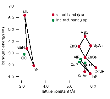
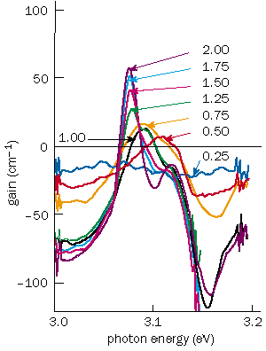
To determine the energy levels responsible for emission and absorption, we measured the light emitted when a current of 20 mA was applied to the structure (electroluminescence) and when monochromatic light was focused on the device (the photocurrent spectrum). Electroluminescence from the blue and green diodes was most intense at 453 nm (2.73 eV) and 520 nm (2.38 eV), as expected from their band-gap energies (figure 4). The largest peak in the photocurrent spectra, at 360 nm, is simply due to the absorption of light by the thick surrounding layers, although there are also weaker shoulder-like peaks at 410 nm for the blue LED and at 420 nm for the green one.
It has since been shown that these smaller peaks result from absorption by free “excitons” in the n = 1 energy level. Excitons are electron-hole pairs held together by the Coulomb interaction, and they form when electrons and holes are injected into the InGaN quantum well.
The energy difference between absorption by the n = 1 quantum energy state and the peak in the electroluminescence signal was 290 meV for the blue LEDs and 570 meV for the green ones. All of the electroluminescence is observed at the lower tail of the absorption spectra, suggesting that light emission results from the recombination of electrons and holes at deep localized states with energies of 290 and 570 meV.
When more indium is included in the active layer, there are larger variations in the indium content, leading to the formation of lower-energy states. Since green diodes are produced by adding more indium, the photocurrent spectrum of the green diode extends to lower energies.
Laser action
We first achieved laser emission from diodes based on III-V nitrides in 1995. These devices were based on multiple quantum wells of indium gallium nitride, and produced blue light efficiently at room temperature. Although early versions required high voltages and could only generate laser pulses, continuous-wave lasers have now been developed. By 1997 the lifetime of continuous blue lasers had improved to 27-35 hours, and the latest research has further extended the lifetime to 10,000 hours. This improvement in lifetime suggests that laser diodes based on indium gallium nitride will soon be commercialized with even longer lifetimes.
The continuous-wave laser diode is made from a layered structure with between 2 and 10 quantum wells. At room temperature, the current needed for laser emission is about 20 mA and the threshold current density is 2-4 kA cm-2, about 10 times higher than in red laser diodes. The operating voltage is 4-6 V, compared with about 2 V for red lasers, while the maximum output power was 50 mW per facet. Most of the light is emitted at wavelengths of 390-420 nm.
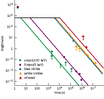
In 1997 Takahiro Deguchi and colleagues at Waseda University in Japan studied how the gain spectra of InGaN laser diodes depends on the power supplied by a pump laser. The sharp peak at 3.07 eV is particularly strong for pump powers in excess of 1 MW cm-2, and marked absorption is observed at 3.15 eV. The absorption is again caused by free excitons in the n = 1 energy level of indium gallium nitride. But the sharp gain cannot be understood in terms of the conventional picture of recombination between conduction and valence bands.
Indeed, the feature only appears when the energy of the pump laser matches the difference in energy between the n = 1 energy level and the energy of deep localized states in the InGaN layer. This suggests that the strong absorption at the n = 1 energy level transfers carriers into deep localized states. Electrons injected into the conduction band of the InGaN quantum well are transferred into localized states, while holes are supplied to the top of the valence band. Stimulated emission therefore takes place between the localized states and valence bands of the InGaN quantum wells. Population inversion is quite easy to achieve because the density of electronic states is expected to be relatively small in the localized states. This means that only a few injected electrons are needed to raise the quasi-Fermi level in the localized state, which increases the energy difference between this level and the energy level at which recombination takes place. Population inversion can therefore be achieved at low currents.

The large lattice mismatch between gallium nitride and sapphire means that up to 1010 dislocations per cm2 can form at the interface, and these defects can thread their way into the active layer (figure 6). In 1995 Steven Lester and colleagues at Hewlett Packard Laboratories in Palo Alto, California, measured a similar density of dislocations in light-emitting diodes based on InGaN.
So why are devices based on indium gallium nitride so efficient? In conventional III-V compound semiconductors, such as gallium arsenide and indium phosphide, the dislocation density must be less than 103 cm-2 to achieve high efficiencies. The presence of indium appears to play a key role, particularly since devices based on gallium nitride are much less efficient. It seems that free excitons formed in the InGaN layer are transferred into the deep localized energy states before they can be captured by the non-radiative recombination centres formed by dislocations. The electrons and holes can therefore recombine to emit blue light, without interference from non-radiative recombination centres. Localized energy states are thus the key to obtaining efficient light-emitting devices based on III-V nitrides.
Into the blue
The advances in light-emitting diodes and laser diodes based on indium gallium nitride have progressed at an amazing rate. It has taken just two years to progress from pulsed to continuous operation of blue laser diodes, while the same advance for conventional laser diodes based on III-V compound semiconductors has generally taken over 10 years.
The recent improvement in lifetimes suggests that blue lasers will soon appear on the market. With so many potential applications, the optoelectronics industry is eagerly anticipating a move into the blue.
Further reading
H Amano et al. 1989 P-type conduction in Mg-doped GaN treated with low-energy electron beam irradiation (LEEBI) Japan J. Appl. Phys. 28 L2112
T Deguchi et al. 1997 Gain spectra in CW InGaN/GaN MQW laser diodes E-MRS (June 16-20, Strasbourg, France) L-XIII-3
S D Lester et al. 1995 High dislocation densities in high efficiency GaN-based light-emitting diodes Appl. Phys. Lett. 66 1249
S Nakamura et al. 1992 Hole compensation mechanism of p-type GaN films Japan. J. Appl. Phys. 31 1258
S Nakamura et al. 1995 Superbright green single-quantum-well-structure light-emitting diodes Japan. J. Appl. Phys. 34 L1332
S Nakamura et al. 1997 High-power, long-lifetime InGaN multi-quantum-well-structure laser diodes Japan. J. Appl. Phys. 36 L1059
S Nakamura et al. 1997 InGaN/GaN/AlGaN-based laser diodes with modulation-doped strained-layer superlattices Japan. J. Appl. Phys. 36 L1568
S Nakamura and G Fasol 1997 The Blue Laser Diode (Springer, Heidelberg)
S Nakamura and T Mukai 1992 High-quality InGaN films grown on GaN films Japan. J. Appl. Phys. 31 L1457