Physicists have built a lens that can image nano-scale objects using visible light

One of the best known properties of light is that it diffracts, bending or spreading around objects that lie in its path. A familiar example is when a collimated beam of light passes through a small aperture in an opaque barrier. If the aperture is large, the light emerges as a beam with the same radius as that of the aperture. But if the size of the aperture is similar to the wavelength of the incident light, the emerging light flares out from the aperture and forms a diffraction pattern whereby the intensity of the transmitted light has a broad central peak.
Diffraction restricts the resolution of microscopes and other optical devices to the wavelength of light used. To see why, imagine two widely spaced apertures that are illuminated by the same beam of light so that each aperture produces its own diffraction pattern. If the apertures are moved closer together, their diffraction patterns overlap until they eventually merge to form a single peak. The individual apertures can then no longer be resolved by observing the transmitted light. This unwanted effect is known as the diffraction limit.
As is often the case in physics, this simple picture is a little more complicated in practice because light that squeezes through a sub-wavelength aperture emerges in two portions. First there is a “far-field” portion that propagates away from the aperture and can be refocused by conventional lenses. Then there is a “near-field” portion that stays put, remaining localized around the aperture over a region less than a wavelength in size.
The near-field portion contains all of the sub-wavelength spatial details about an object, but it decays quickly as a function of distance from the object. Conventional optical devices are therefore unable to convey these finer details to an image. Instead, such instruments are constrained to recover as much of the far-field light as possible, limiting their resolution to roughly the wavelength of light.
But if a “perfect” lens existed that could recover all of the near-field and all of the far-field light, then an exact image of the object could be formed with perfect resolution. Even if the lens could recover only a fraction of the near-field light it would still produce an image with a resolution that would be well beyond what is currently possible. Two independent teams have now managed to build such a lens – dubbed a “superlens” – from a thin layer of silver. Their lenses, which work with visible light, can be used to image structures with a resolution as high as one-quarter the wavelength of the incident light.
Superlenses in theory and practice
The idea of a lens that can beat the diffraction limit was first proposed by John Pendry of Imperial College, London, five years ago. To the eye, Pendry’s superlens would look like nothing more than a thin planar film of material. However, there would be one crucial difference: the lens would have a negative refractive index. Pendry found that if the value of the refractive index, n, were just right (usually about −1) then the superlens could focus not just the far-field light but also some of the near-field light. This would not be possible if the material had a positive refractive index.
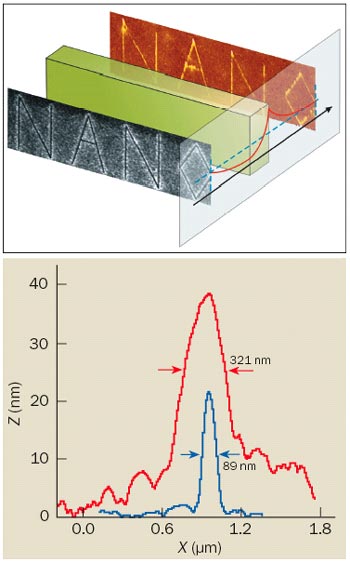
The near-field light can be pictured as a collection of “evanescent” waves that decay exponentially with distance from source. The waves that decay fastest convey the smallest spatial features, which means that the resolution of the image can be improved by detecting as many of the evanescent waves as possible. Pendry’s superlens would do this by reversing the decay of the evanescent waves, causing them to grow exponentially as they pass from one side of the superlens to the other, where they would decay once again and be recovered at the image plane (see figure).
So how do you build a superlens? Unfortunately, nature does not provide us with materials that have a negative refractive index. But nearly 40 years ago the Russian physicist Victor Veselago postulated that such a material could exist in theory, provided that its electric permittivity, ε, and magnetic permeability, μ, are both less than zero. The material’s refractive index, which is defined in this case as n = −√(εμ), would then also be less than zero. However, physicists had to wait until 2000 before an artificially structured composite material with a negative refractive index was developed for the first time. The material was designed so that both ε and μ were less than zero over certain microwave frequencies.
This breakthrough triggered an explosion of interest in the properties of artificial negative-refractive-index “metamaterials”. But although they can easily be designed to operate at lower frequencies, it is difficult to make such materials small enough to operate with visible light. In separate recent experiments, Steve Brueck and colleagues from Columbia University, and Vladimir Shalaev and colleagues from Purdue University managed to make nano-patterned structures that have a negative index at wavelengths of 1.5-2 μm, which is almost in the visible region of the spectrum. Unfortunately, these particular structures absorbed a lot of light and thus are not yet good candidates for a superlens.
While many materials have a negative electrical permittivity at optical wavelengths, it is not easy to ensure that μ < 0. To get round this problem, Pendry noted that a planar slab of material with ε = −1 could act as a partial superlens even if μ itself is positive. The material would then recover enough of the near-fields to beat the resolution of any conventional lens.
The two new experiments – one by Xiang Zhang and co-workers at the University of California at Berkeley (N Fang et al. 2005 Science 308 534) and the other by Richard Blaikie’s group at the University of Canterbury in New Zealand (D Melville et al. 2005 Optics Express 13 2127) – have independently confirmed the phenomenon of superlensing in the context of optical lithography. This new work comes on the heels of a demonstration of superlensing in a guided-wave structure at microwave frequencies by George Eleftheriades and colleagues at the University of Toronto, reported last year (see “Beating the diffraction limit” Physics World May 2004 pp23-24).
Great pictures
Both new experiments involve building a superlens from an evaporated thin silver film, the thickness of which is carefully selected to optimize the refocusing of evanescent waves (30-50 nm). This thickness is a trade-off; make the lens too thick, and losses start reducing the resolution; make the lens too small, however, and the experiment becomes impractical because the object has to placed at least a distance of d/2 from the centre of the lens, where d is the thickness of the film. Silver is a convenient choice for the superlens because it has relatively low losses at optical wavelengths. Moreover, ε = −1 for silver at ultraviolet wavelengths, where optical lithography and imaging can easily be performed.
To demonstrate superlensing, the two teams had to fabricate all of the essential elements of an optical system. These included an object, a dielectric spacer layer to provide an adequate working distance, the superlens itself, a further dielectric spacer layer and finally an image plane. The object in these experiments was not a lump of material, but instead was the light passing through various lines etched onto an opaque tungsten or chromium mask. The problem with imaging an object such as a piece of silicon is that you would have to find a way of illuminating the silicon while rejecting the incident light, which would be tricky. Here, the researchers did not have to worry about this because the mask blocked all of the unwanted light.
The features of the mask were written using either an electron or an ion beam, both of which create lines that are narrower than the 365 nm wavelength used for imaging. To view the image, a layer of photoresist was placed where the image was expected to form. The light from the mask exposes the photoresist, creating a sub-wavelength lithographic pattern that can then be imaged later, for example with an atomic force microscope.
The light that passes through the object mask undergoes diffraction. But if the superlens is inserted between the object mask and the image plane, then the resolution of the image is significantly improved due to the refocusing of evanescent waves. Blaikie and colleagues illustrated this improvement by comparing images of patterned gratings with progressively smaller periods. With the superlens present, gratings with periods as small as 120 nm – one-third that of the illuminating wavelength – could be imaged.
In addition to gratings, Zhang and co-workers also patterned the word “NANO” onto a mask, with each of the lines in the letters having a width of 40 nm. In the absence of the superlens, the pattern formed a fuzzy image at the image plane, with the imaged linewidths being roughly 320 nm. With the superlens in place, however, the image was considerably sharper, with the linewidths less than 90 nm – one-quarter of the incident wavelength.
The price of perfection
These two experiments demonstrate the phenomenon of evanescent-wave refocusing and prove that the superlens is much more than a theoretical curiosity. But superlensing does come at a cost because the object, lens and image are all very close together, spaced over a distance considerably less than one wavelength. In other words, to image the near-field it is necessary to remain in the near-field, otherwise those components of light that contain the sub-wavelength spatial details decay to the point that they cannot be recovered.
Still, the superlens is a conceptually new and intriguing device that has already altered long-held notions of optics. Moreover, superlensing may find practical applications in industries such as optical lithography or optical storage, where, among other things, it will enable manufacturers to fabricate devices on smaller scales.


