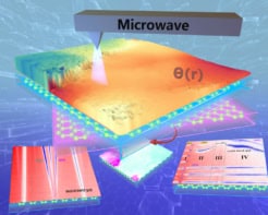
Wafer-thin sheets of silicon are increasingly being used in "silicon-on-insulator" (SOI) technology, in which electrically conducting silicon films are laid down on top of a thick slab of insulating silicon dioxide. But as researchers strive to make the films ever thinner, they worry that imperfections in the silicon could trap mobile charge carriers -- electrons and "holes" -- at the interface between the two materials and so prevent the material from conducting. Now, however, scientists in the US have found that silicon layers just 10 nanometres thick can conduct electricity efficiently after all, provided their surfaces are clean (Nature 439 703).

SOI technology is interesting because it could be used to build new types of high-speed electronic circuits and sensors. But many of the foreseen advances depend on making the silicon layer as thin as possible. The danger is that if the silicon gets too thin, it no longer behaves like bulk silicon. Researchers have thought that charge traps at the interface with the silicon dioxide could deplete the silicon layer of free carriers and make the resistivity far too high.
One way of telling if the resistivity is too high is if measurements that depend on the flow of current, such as tunnelling microscopy, are impossible with silicon-on-insulator structures. Now, however, Paul Evans and colleagues of the University of Wisconsin-Madison and Soitec in the US have been able to use this technique to image a 10 nm-thick boron-doped silicon layer supported on a silicon dioxide substrate. The only proviso for conduction is that the different layers have to be clean.
“This tells us that if you’re building nanostructures, the surface is really important,” says Evans. “If you make silicon half as thick, you would expect it to conduct half as well. But it turns out that silicon conducts much worse than that if the surface is poorly prepared and much better than that if the surface is well prepared.”
The team believes that the cleaning process creates new electronic states on the silicon surface. These surface states interact with the “bulk” band structure of the silicon, enabling high-mobility carrier conduction and boosting conductivity.


