An international team of physicists has created the first semiconductor material in which the width of the energy gap between the valence and conduction bands can be changed by simply applying an external voltage.
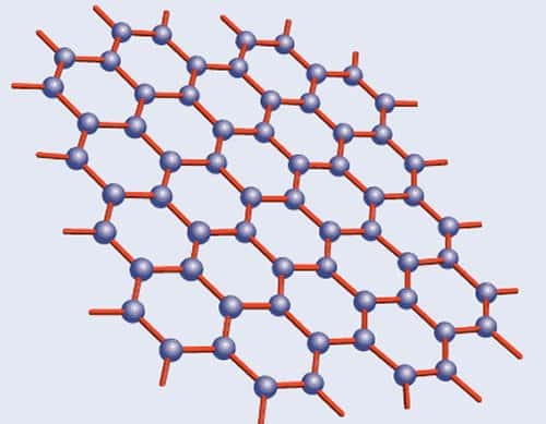
The material is a “graphene bilayer”, which is made of carbon and is only two atomic layers thick. The team claims that the semiconductor could be used to make transistors, lasers and other devices with properties could be much more easily tuned than devices based on traditional semiconductors such as silicon.
Semiconductors are useful because they can be used to switch electrical currents on and off. This is done by applying a small voltage to the semiconductor, which promotes electrons across the energy gap between the valence and conduction bands. However the width of this gap – and hence the switching voltage – is an intrinsic property of the semiconductor and can only be changed my modifying its chemistry, structure or both.
A semiconductor with a “tuneable” gap that can be changed externally – by applying a voltage, for example – could lead to new types of electronic devices, notably lasers where the wavelength of the light could be dialled-up with great precision.
Gapless semiconductor
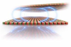
Now, however, Antonio Castro Neto of Boston University, along with colleagues in the US, Portugal, Spain and the UK, have been able to make a tuneable semiconductor from graphene (Phys Rev Lett 99 216802). This material, which consists of a thin sheet of carbon just one atom thick, normally has no gap between its valence and conduction bands. But by placing two layers of the graphene on top of each other to create a bilayer, an energy gap is created if the material is placed between positive and negative electrodes.
According to a theory developed by the team, the gap arises because the transverse voltage causes an excess of negatively charged electrons in one layer and an excess of positively charged “holes” in the other layer. These electrons and holes are believed to pair up to create quasiparticles, which behave differently than their constituent particles.
A peculiar feature of electrons and holes in graphene is that they move through the material as if they have no rest mass – something that makes the material a very good conductor. However, the quasiparticles have a rest mass and according to Castro Neto, this mass leads to an energy gap that must be overcome before current can flow.
The team measured the quasiparticle mass in a graphene bilayer ribbon that was about one micrometre wide and several micrometres long. The graphene was mounted on an oxidized silicon wafer and a voltage was applied between the silicon and an electrode above the graphene.
Cyclotron resonance
A magnetic field was also applied to the bilayer, which caused the quasiparticles to move in circular orbits – an effect called cyclotron resonance. The team measured the period of this resonance, which depends on the mass of the quasiparticles. The team discovered that this cyclotron mass increased as the applied voltage increased from zero to about 100 V, allowing them to conclude that the energy gap was also changing from zero to about 150 meV.
Castro Neto told physicsworld.com that graphene semiconductors could someday be used to make new types of transistors, lasers and molecular sensors in which the energy gap could be changed at will. This property, when combined with graphene’s small size, great mechanical strength and high thermal and electrical conductivity, make it look very attractive as a replacement for traditional semiconductors such as silicon.


