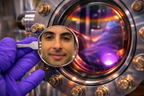
Compound semiconductors like gallium arsenide (GaAs) could bring a revolution in optics and electronics, with the promise of highly efficient solar cells and a new generation of components. The trouble is that devices made from these materials are difficult to produce and their delicate nature leaves them prone to damage. But now a group of researchers based in the US and South Korea has designed a new assembly technique, which they say could produce these materials en masse and integrate them into devices with relative ease. They demonstrate their technique by producing a number of rudimentary electronic components.
While silicon is still the dominant material in many hi-tech industries, compound semiconductors could hold big advantages for certain applications. This is on account of the high mobility of electrons within the materials and their direct band gaps, which make them particularly effective at manipulating light. But the problem facing the compound-semiconductor industry is that they are competing with a market dominated by silicon with its established manufacturing base that is incompatible with compound semiconductors.
Printing technique
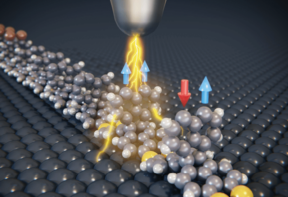
Now, John Rogers, working with colleagues at the University of Illinois at Urbana-Champaign and a related company, offer a production method by adapting a transfer-printing technique that they have been developing for the past few years. They begin by growing stacks consisting of multiple layers of gallium arsenide and aluminium gallium arsenide, which they then “peel” off one-by-one using a silicone-based stamp. The layers detach easily on account of van der Waals forces, which are stronger on the stamp surface than between layers of compound semiconductor. The researchers then stamp these individual flakes to target sites on a silicon wafer.
To demonstrate the precision and robustness of its technique, Rogers’ team creates three well-known components: field-effect transistor with logic gates; near-infrared (NIR) imaging devices and photovoltaic modules. The scientists use the NIR to show the full detail of the devices.
The research group intends to develop its research by developing more complicated component, including detectors for solar cells. The advantage of using direct band-gap materials like this is that incoming photons can easily form liberate electrons, which can then be collected as current. In silicon-based solar cells, the band gap is indirect so electron–hole pairs will only form if a lattice vibration known as a phonon – with the right momentum – is available.
Practical challenges
“Our biggest opportunity is in solar cells, where compound semiconductors haven’t been competitive so far,” says Rogers. He also believes that there is a compelling opportunity in other optoelectronic applications, such as highly efficient switches.
Chris Phillips, a semiconductors researcher at Imperial College London says that he welcomes this kind of practical approach to compound-semiconductor research. However, he warns that there are still major practical challenges to address regarding the “flimsy” nature of these materials. “With conventional semiconductors, the action is deep within the crystal. In these thin flakes, the layers could easily become dislocated leading to electron-hole recombination and severe reductions in efficiency,” he says. Philips feels that the biggest opportunities for compound semiconductors will be with hybrid devices where new materials can be integrated into silicon-based circuitry.
This research is published in Nature.