With a focus on parallel optimization and nanoscale accuracy, precision positioning specialist PI is streamlining the optical alignment, test and packaging of quantum photonic devices

The future of photonics is taking shape along two converging coordinates as on-chip optical integration meets next-generation quantum technologies that exploit the exotic properties of quantum mechanics – entanglement, tunnelling, superposition and the like. The end-game: integrated quantum photonic devices, produced at scale, to controllably manipulate the quantum states of optical materials, opening the way to practical applications like quantum computing, quantum communications, quantum metrology and quantum imaging.
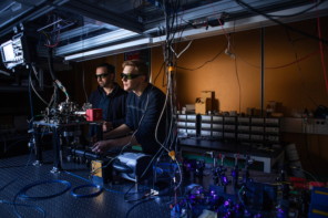
To make that quantum vision a reality – initially in an R&D context, though ultimately in terms of volume production and manufacturability – the German precision motion specialist PI (Physik Instrumente) has addressed a vexing, costly and long-term bottleneck in the testing, characterization and manufacturing of photonic devices down to the atomic scale.
Here Scott Jordan, head of the photonics market segment for PI, tells Physics World how the company’s Fast Multichannel Photonics Alignment (FMPA) technology – a set of firmware-level commands built into the vendor’s digital nanopositioning controllers, intelligent microrobots and stage controllers – can help developers to automate the optical alignment, test and assembly of quantum photonics devices while driving down production costs.
Why is automated active alignment – the foundation of FMPA – so important for the assembly of photonic devices?
There are growing requirements to align and position multiple optical components – for example, the lenses in smartphone cameras or the CCD chip itself – with nanoscale accuracy and economic efficiency. In integrated silicon photonics and next-generation quantum photonics, a multitude of tiny active and passive optical devices must be aligned for testing and packaging, starting at the wafer level. The common theme is multiple channels, multiple elements, multiple interacting inputs and outputs, multiple degrees of freedom – all need to be aligned and optimized multiple times throughout the manufacturing process.
If this is the problem, FMPA technology is part of the answer. Put simply, aligning the inputs and outputs of integrated photonic devices at industrial pace requires parallel optimization and nanoscale accuracy – not least in the coupling of on-chip waveguides with optical fibres. As we move into the quantum photonics realm, with its more complex production and test requirements, this parallelism will become increasingly critical to the process economics.
It sounds like the parallelism offered by FMPA has been a game-changer in photonics R&D and manufacturing?
FMPA is a huge advance over previous automated alignment technologies. Optical alignment is the single biggest cost/time sink in the testing and packaging of integrated photonic devices. In the short waveguides, typically millimetre-scale or less as increasingly deployed in silicon photonic devices, the input and output couplings can steer each other – so as one side is optimized, the other shifts slightly and needs reoptimization. In the past, this necessitated a time-consuming, serial sequence of back-and-forth adjustments of the input, then the output, repeating and iterating towards a global consensus alignment.
Similarly, when optimizing an angle, the transverse alignment would be impacted and would conventionally need to be reoptimized, again in a time-consuming serial loop. With FMPA, these interacting alignments can be optimized simultaneously to deliver a global consensus alignment, often in one go. In many cases, tracking and continuous optimization of all the alignments is also possible, allowing compensation of drift, curing stresses, and so on.
At a fundamental level, how do PI’s intelligent microrobots deliver optical alignment?

At PI we make precision motion and nanopositioning technologies. Over the past four years, we have implemented a new generation of algorithms in the controllers for this equipment. These algorithms intelligently seek the optimum of a given optical figure of merit versus position. There are two types of alignment process: area scans to localize the main peak for a given parameter (e.g. optical power, modulation transfer function or modal purity) within a defined region, while parallel gradient searches efficiently optimize one or more such couplings at once – and optionally track them to mitigate drift processes and positional disturbances caused by temperature changes. In the case of a coupling between an on-chip waveguide and an optical fibre, for example, the manufacturer typically wants the alignment to minimize the light loss going from one element to another.
How have PI’s customers responded to FMPA technology?
The commercial launch of our parallel alignment technology was well timed. When we introduced FMPA four years ago, we found a niche with research and industry customers searching for faster optical alignment solutions to improve their production and test economics. A big driver is silicon photonic devices with arrayed-waveguide inputs and outputs – multiple optical channels that must be aligned simultaneously with optical fibres or other elements. To meet that need, we now have leading industrial players in silicon photonics – the likes of FormFactor Inc in the US, MPI in Taiwan and Tegema in the Netherlands – building high-throughput test and assembly equipment – photonic wafer probers and packaging-automation tools, respectively – based on our microrobots, positioning stages and advanced controls technology.
So FMPA is already being exploited to support early-stage device R&D in quantum photonics?
Absolutely. FMPA is at the heart of leading-edge photonic wafer probers that are being deployed by industry for testing of prototype quantum photonic devices – as well as optimizing the fabrication processes for such quantum devices. The probers are used to test the electronic and optical functionality of each photonic device on the wafer, so that the developer knows which devices are worth packaging. The same functional elements are routinely deployed on the benchtop level as well.
Is FMPA also being used by academic researchers working on quantum photonics?
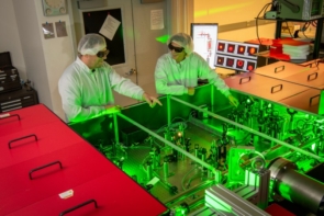
We work with many pioneering academic customers to support development of next-generation quantum photonic devices. A case in point is a team led by Vlad Shalaev at Purdue University (West Lafayette, IN), who are using our FMPA systems to map, track and characterize novel single-photon quantum emitters that could prove fundamental to photonic implementations in quantum computing.
Essentially, the Purdue team has demonstrated high-brightness, single-photon quantum sources operating at room temperature – creating streams of fully randomized photons from atomic defects in nanoscale diamond films. To make use of the photons created by these defects, however, it is first necessary to collect them, guide them down an optical fibre, and measure them using a photon counter (typically tens of thousands of photons per millisecond).
With this in mind, we helped them build an open-source FMPA workstation comprising a very-high-precision xy positioning stage with an aperture in the middle – a set-up that is used to scan and lock onto the atomic-scale emitters so that they can be characterized. The workstation software took only eight hours to build from scratch, largely because all the functionality is incorporated into our motion controllers. All in, a neat example of PI’s alignment technologies being put to work in a fundamental research context that has demonstrated some world-leading results.