A superior class of nitride laser is on the cusp of commercialization thanks to the development of novel mirrors and radical current-injection schemes, as Richard Stevenson reports
What is the most valuable attribute for a laser? Some would argue in favour of efficiency, so that the laser can run off a battery. Others might prefer a device that can turn on and off at high speeds, so it can transmit vast amounts of data. There are also those who place a premium on a circular emission profile, simplifying the focusing of the beam, or argue that what matters most is compatibility with low-cost, high-volume manufacture.
Ticking all these boxes and more is the VCSEL – the vertical cavity, surface-emitting laser. First proposed by Kenicha Iga from Tokyo Institute of Technology in 1977, this class of semiconductor laser is also renowned for its temperature stability, as well as the very low current required to turn it on. Its more common edge-emitting cousin, which is used in CD and Blu-Ray players, long-distance fibre-optic networks, and welding and cutting tools, shares few of these attributes, which is now starting to make electronics manufacturers take notice. Even if you haven’t heard of the VCSEL, there is a good chance that you own a few of them: the iPhone X’s three VCSEL chips play a key role in its facial recognition system. Before iPhones became the killer application, data centres provided the biggest market, with VCSELs deployed in short-reach communication. Both sectors are helping to drive up sales. According to market analyst Yole Développement, global sales revenue reached almost $700m in 2017, and will swell to $3.5bn by 2023.
Sales could go even higher, though, if the VCSEL can expand its spectral range. Today’s commercial offerings are restricted to the red and the infrared. If VCSELs could emit in the blue and green region of the spectrum, they could be used for high-resolution printing, high-density optical data storage, and chemical and biological sensing. What’s more, the combination of red, green and blue VCSELs would make it possible to use these chips in full-colour displays and lighting. Although output power requirements for the VCSEL vary by application, a useful ballpark figure is 10 mW – enough for augmented reality devices, projection systems and displays. The good news is that after more than a decade of hard-fought progress in both industrial and academic labs, this benchmark has now been met for blue VCSELs, thanks to innovations in the device’s architecture and its fabrication processes.
Getting the blues
Given the success of infrared and red VCSELs, the “obvious” road to developing blue and green cousins was to retain as much of their design as possible, while shifting the wavelength. Unfortunately, the “obvious” road turned out to have some considerable bumps.
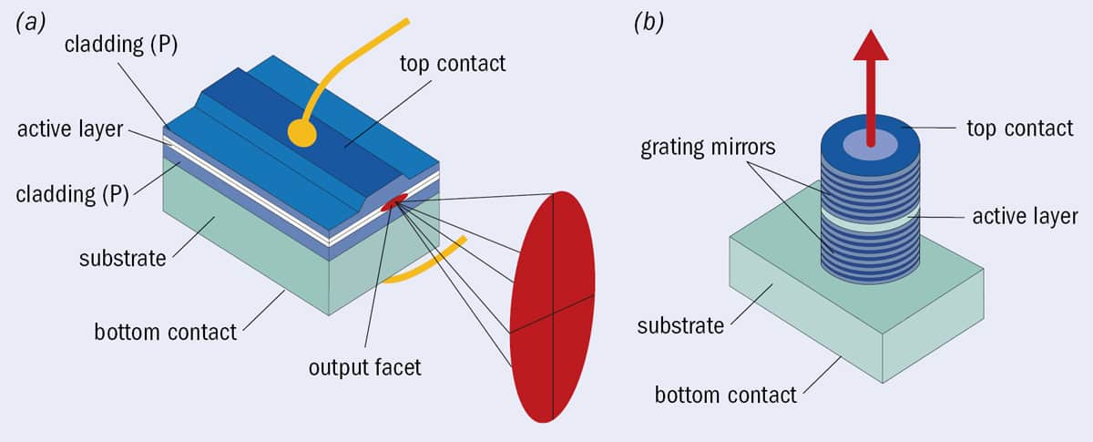
Lying at the heart of every laser is its cavity, where light is generated and amplified to produce stimulated emission. This cavity is bookended by a pair of mirrors, providing optical feedback – a prerequisite for lasing. In a VCSEL, the cavity is just a few microns thick, hundreds of times thinner than typical cavities in edge-emitters (figure 1a). Such a short cavity enables the device to turn on and off very quickly, but the penalty is that the mirrors need to be highly reflective for lasing to happen.
The process of making infrared and red VCSELs begins by taking a thin disc of crystalline gallium arsenide (GaAs) and growing on top of it alternating layers of GaAs and (depending on the emission wavelength of the laser) either aluminium arsenide (AlAs) or the alloy aluminium gallium arsenide (AlGaAs). This stack of layers acts as the first mirror. The cavity that contains the light-emitting region is then added, followed by the layers that make up the second mirror (figure 1b). To define precisely where the light comes out of the VCSEL, a circular aperture is constructed by selectively oxidizing, from the outside in, an aluminium-rich layer below the top mirror. The process continues until only a non-oxidized hole, with a diameter of a few micrometres, remains. As this hole is the only part of the layer that can pass a current, the local current density rises high enough for lasing to begin.
A crucial detail of the VCSEL’s construction is that each layer in the mirror stacks must have a thickness equal to one-quarter of the lasing wavelength. This requirement (and the π-phase change that occurs when light reflects off an interface with a higher refractive index material) ensures that all the light that arrives back at the cavity has the same phase, regardless of which part of the mirror provided its reflection. Constructive interference results, supporting lasing of the VCSEL. The pairing of GaAs and either AlGaAs or AlAs is a good one in this respect because the materials’ refractive indices are very different. This means there is substantial reflection at interfaces within the mirror, and 20 or so layer pairs per mirror are enough to reflect 99% of the light.
Unfortunately, the arsenides, which are also used to make countless red LEDs and edge-emitting lasers, are incapable of emitting light at much shorter wavelengths. The obvious solution for making blue and green VCSELs is to replace them with nitrides – the material system used for making blue and green LEDs and edge-emitting lasers. All teams developing blue and green VCSELs have adopted this approach, but it comes with certain drawbacks. In particular, the refractive indices of the nitrides are relatively similar. Getting sufficiently reflective mirrors therefore requires roughly twice as many layers, leading to an unacceptably long time for growing the entire device structure.
Dielectric delights
Recognizing this, Nicolas Grandjean, who heads a group at EPFL, Switzerland, that pioneered nitride VCSELs, chose to replace the top mirror with one formed from a pair of dielectric materials with a significant refractive index contrast. By making this top mirror from a combination of silicon nitride and silicon dioxide, Grandjean and his colleagues trimmed the number of layer pairs in this mirror to just 16.
Even with this modification, fabricating the device is far from easy. That’s partly because the task of growing the bottom, nitride-layer mirror for blue and green VCSELs is more challenging than the equivalent task in arsenide-based devices. Atoms in the crystalline structures of AlGaAs and GaAs are spaced almost the same distance apart, so when one material is grown on the other, there is no build-up of strain in the structure. That’s important, because, left unchecked, strain can generate performance-impairing defects.
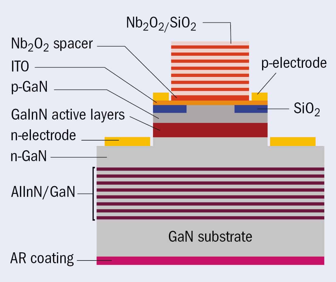
To stop strain building up in nitride layers, Grandjean and co-workers paired GaN with the alloy aluminium indium nitride (AlInN), which is lattice-matched to GaN in the form Al0.83In0.17N. Growing a uniform film of this material is not easy, but Grandjean’s team identified conditions for producing good quality AlInN before building their VCSELs. Their design, which has an aperture formed by oxidizing AlInN, also featured a novel approach to injecting current into the device. In a conventional VCSEL, current flows through the mirrors. But dielectric mirrors don’t conduct, so they added electrical contacts to either side of the cavity.
Humble beginnings
The work of Grandjean’s team was carried out more than a decade ago, and the high point came in 2007, when they demonstrated lasing in a blue VCSEL pumped with an argon-ion laser. However, when their VCSEL was driven electrically – the mode of operation required for a practical device – they were only able to extract non-coherent light from it. Further progress would have required additional refinements to the fabrication processes, but funding for such work was unavailable in part because decision-makers argued that the necessary breakthroughs would come via work being done in Japan, where researchers pioneered light-emitting nitride devices in the 1990s.
Broadly speaking, they were correct: much of the subsequent progress in VCSEL development has indeed come from scientists at Japanese electronics firms. However, other groups have also made valuable contributions. Among them is a team from National Chiao Tung University, Taiwan, which reported the first electrically driven nitride VCSEL in April 2008. To coax laser light out of their device, the researchers cooled it with liquid nitrogen. This is not practical for a commercial light source, but further progress came later that year when researchers at the Japanese firm Nichia produced the first blue VCSEL capable of operating at room temperature. Appropriately enough, Nichia is where Shuji Nakamura, who shared the Nobel Prize for Physics in 2014 for developing blue LEDs and is also credited with inventing the blue laser diode, spent much of his career.
Nichia’s design broke new ground, dispensing with nitride mirrors altogether. However, it’s debatable whether this made its VCSEL easier to fabricate. After the cavity was grown, it had to be removed from the substrate that provided the foundation for its growth and then carefully polished to a very precise thickness, defined by the lasing wavelength. Despite this, Nichia persisted with the design, and in 2009 engineers announced that they had increased the laser’s output from 0.14 mW to 0.62 mW by switching the substrate from sapphire to GaN. This change improved material quality, slashing defects by three orders of magnitude.
Unfortunately, the Nichia team also found that after just 10 minutes of operation, the minimum current needed to turn on their devices started to drift – perhaps because of mechanical stress induced in the GaN wafer during the polishing process. The company reported a modest improvement in the output power of its blue VCSEL in 2011, but it has not published any papers on this topic since 2012, suggesting that its process has significant issues.
Milliwatt milestones
It took several years, and yet more innovation, to produce the first VCSEL with an output power of 1 mW or more. Sony claimed this milestone in 2016 with a 1.1 mW blue VCSEL produced with a process that begins by forming islands of dielectric mirrors, before growing GaN material between and then over them, and finally depositing the cavity. After this, a second dielectric mirror is added.
More recently, Sony’s engineers unveiled a new design that has broken the 10 mW barrier. It features a far larger cavity and a curved mirror, formed by etching the backside of the substrate and depositing a dielectric stack on this surface. In November 2018 team spokesperson Tatsushi Hamaguchi announced that they had achieved an output power of 12 mW for their blue-emitting VCSEL. At the Photonics West conference in San Francisco, US, a few months later, Hamaguchi revealed a further increase, to 15.4 mW.
Sony’s high-power design has competition in the form of a blue-emitting VCSEL based on an architecture that shares several features with EPFL’s early work. In 2017 researchers at Meijo University and Nagoya University in Japan used a dielectric top mirror and a bottom mirror containing AlInN to construct a VCSEL with a 4.3 mW output. They reported their progress at the International Workshop on Nitride Semiconductors in Strasbourg, France, and Grandjean, of EPFL, called it an impressive result. “The secret is with the growth conditions,” he says. “They can grow at a high temperature and faster, so they improve both the quality of the material and the growth time.”
Since then, Tetsuya Takeuchi and his team from Meijo University have partnered with engineers at Stanley Electric, a Japan-based electronics firm that supplies headlamps to car manufacturers such as Honda and Nissan. Their goal is to increase output power still further, so that Stanley can replace the LEDs in its headlamps with VCSELs. In early 2018 the partnership revealed that it had hit 6 mW by trimming internal loss, and in autumn of the same year the scientists reported that they had exceeded 15 mW by lengthening the cavity and quashing thermal resistance. The latest figure in the public domain is 22.2 mW, announced at the 2019 Photonics West, where team members attributed the increase in power to having optimized the reflectivity of the top mirror.
It’s not easy being green
Replicating these advances for green VCSELs has so far proved difficult. In blue and green LEDs and edge-emitting lasers, light is generated in very thin layers of InGaN, known as quantum wells. Green emission requires more indium in the wells, but this increases the strain, generating defects and impairing performance. Compounding matters, the in-built electric field in this material system increases in strength with indium content, hampering the light-generation process.
To sidestep these issues, a partnership in China between researchers at Xiamen University and the Chinese Academy of Sciences, Suzhou, has turned to quantum dots. The advantages of this move, which include reductions in strain and internal electric field strength, have enabled the fabrication of VCSELs that span the entire green spectral range. So far, the output powers are lagging their blue siblings. However, with the latter now on the cusp of commercialization, funding for green GaN VCSELs is sure to grow, spurring this impressive light source to span a wider spectral range and serve even more applications.
- Enjoy the rest of the 2019 Physics World Focus on Optics & Photonics in our digital magazine or via the Physics World app for any iOS or Android smartphone or tablet.
![]()
Physics World’s Laser at 60 coverage is supported by HÜBNER Photonics, a leading supplier of high performance laser products which meet the ever increasing opportunities for lasers in science and industry. Visit hubner-photonics.com to find out more.