“Industry is not going to accept mechanical exfoliation as a path forward for manufacturing these devices,” says Joshua Robinson, Associate Professor of Materials Science and Engineering at Penn State University in the US. This conclusion is informed by over a decade working in the 2D materials research community, and in particular the past two years spent preparing a roadmap on electronic grade 2D materials, largely led by his graduate students Natalie Briggs and Shruti Subramanian.
Mechanical exfoliation refers to the fabrication approach Andre Geim and Kostya Novoselov used in the first experiments on isolated graphene. At the time researchers would routinely recover a pristine graphite substrate surface for their experiments by removing the top layer with a bit of sticky tape and throwing it away. The curiosity to investigate these discarded scraps one Friday night, thereby revealing a host of wonder properties in the single atomic layer of carbon – graphene – earnt them the Nobel Prize in 2010.
Graphene and 2D materials remain the subject of multibillion euro research across the world. Yet while mechanical exfoliation can yield high quality graphene that is useful for research purposes, fabrication techniques with more scope for industrial scaling than a bit of sticky tape are critical to gaining economic returns on research investment.
Beyond sticky tape
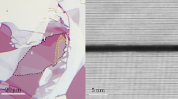
In terms of scale and cost progress in industrially viable fabrication methods has been great. The past decade has seen the cost of graphene plunge from the hundreds of thousands of US dollars per kilogram of graphene at the time it was first isolated to around just 50 US dollars per kilogram. The snag is that graphene from most of these more scalable fabrication methods is prone to defects, which although they may not greatly affect the material’s mechanical properties, significantly compromise the material’s electronic properties.
“2D materials constitute an entire zoo of materials, and within those types of materials are widely ranging qualities – 2D materials for mechanical properties or in composites you want defects so they interact,” Robinson tells Physics World. “In electronics you either don’t want defects or if there are defects we want to know they are very controlled and purposely put there. Random defects do not help us.”
Over the past couple of years there have been various initiatives to help manage this “zoo” of materials, such as the ISO Graphene Standard, an internationally recognized definition of graphene, and the Graphene Service, which offers characterization and advice for graphene users to match materials to suitable applications. When it comes to electronic applications a lot of the graphene produced simply does not hit the grade.
Hope for electronic grade 2D materials
Consequently, Robinson agrees with those who suggest that applications exploiting the more forgiving mechanical properties of 2D materials have a head start in making their way into high street products. However he adds, “There’s been a lot of improvements in the past couple of years – looking at chemical vapour deposition (CVD) and molecular beam epitaxy (MBE) – these are some of the approaches that are going to grow electronic grade 2D materials, so we thought it was time to ask what are the number one challenges that we have to address so that these 2D materials can make an impact.”
The roadmap recently published in the journal 2D Materials outlines a series of applications of electronic grade 2D materials including electronics, Internet of Things devices, computing and solar energy, highlighting the potential for commercial progress and the remaining challenges in both theory and experiment for understanding and mastering the fabrication techniques required.
Taking graphene from wonder material to real-world technologies

Standing on the shoulders of silicon
Robinson also points out how techniques for fabricating electronic grade 2D materials are largely compatible with existing semiconductor fabrication techniques, which as he suggests is arguably the number one reason why their fascination has been so persistent in industry.
“For quantum dots, nanowires and nanotubes you have to put them on a surface by spin coating etc and it’s hard to do this deterministically,” says Robinson. “The key with 2D materials is you can grow them directly on a substrate and use the same processes to make devices as developed with silicon. Manufacturers of semiconductor devices can utilize the same techniques without major changes to their fabrication lines.”
This CMOS-compatible manufacture strengthens the potential for exploiting 2D materials to augment, complement or enhance existing semiconductor technology. In fact Robinson is more than sceptical of the chance of 2D materials – or anything else – replacing silicon in the next 10-20 years, favouring instead a scenario where 2D materials develop alongside conventional electronics.
Could they match the ubiquity of silicon technology in the next decade? Robinson suggests they may have a greater impact in some areas than others, promising avenues being the post-fabrication processes in transistor technology, sometimes described as Back-End-Of-the-Line (BEOL), and certain computer memory technologies.
“I think one of the big things is being able to do the manufacturing in a manner that is compatible with silicon technology and that is the real trick for the things we are trying to do,” says Robinson. “This roadmap is focused on how to make these materials electronics grade because if we can’t make them high enough quality – controlled properties low defects etc – they will never be ubiquitous even if the intrinsic properties are revolutionary.”
The full roadmap is available in the journal 2D Materials.