Since the discovery of graphene over two decades ago now, two-dimensional (2D) materials have revolutionized almost all areas of science and technology thanks to their unique properties compared with bulk materials. These include high electronic conductivity, high mechanical strength, transparency and flexibility, to name just a few. The problem since the beginning, however, has been to produce sheets of these materials large enough for real-world applications and, importantly, to be able to transfer them onto other substrates without cracking the sheets. A team of researchers in Amsterdam, the Netherlands, has now succeeded in doing just this, with the help of an unexpected material – kitchen cling film. Their work could help in the continuing development of next-generation electronic and optoelectronic devices.
“The method we developed allows us to, for the first time, pick up, transfer and place large (roughly 1-mm-sized) 2D layers on almost arbitrarily patterned surfaces,” explains Jorik van de Groep of the 2D Nanophotonics group at the UvA-Institute of Physics, who led this research study. “Being able to do this is crucial since it enables the integration of 2D materials with structures like larger electronic devices and photonic coatings. Most importantly, the transfer is no longer probabilistic (as were most other methods) but has a near-unity yield.”
In the early days of 2D materials, researchers obtained micron-sized mono- or multi-layers of these structures by mechanically shaving off, or exfoliating, flakes from the bulk material using sticky tape. This was first famously done for graphene, a sheet of carbon just one atom thick. More recently, a technique known as gold-assisted exfoliation has allowed them to produce high-quality centimetre-sized layers of technologically important materials like transition-metal dichalcogenides (TMDCs) and transfer these onto flat glass surfaces.
For the field of nanophotonics in particular, explains van de Groep, we need to be able to transfer large-area 2D materials onto both flat and patterned substrates – such as those with electrical contacts and optical coatings on them, for example – if we are to fabricate functional devices. The problem is that existing transfer techniques are limited in this respect.
Kitchen cling film to the rescue
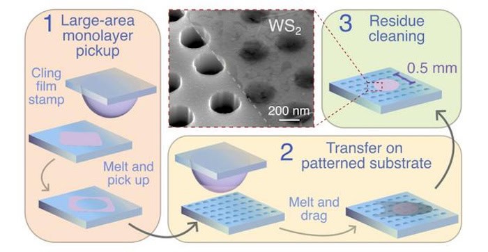
The Amsterdam team – which also includes researchers from UvA’s Van ‘t Hoff Institute for Molecular Sciences, ARCNL and AMOLF – has now developed a simple method that allows them to reliably transfer both large-area monolayers of TMDCs and hexagonal boron nitride/monolayer heterostructures onto patterned or non-patterned substrates, ranging from flat surfaces to high-aspect ratio and low adhesion patterned interfaces. In their process, which is detailed in ACS Nano, they used low-density polyethylene (LDPE), or kitchen cling film, an inexpensive and widely available polymer that has a low melting temperature.
In their work, the researchers transferred a gold-assisted-exfoliated large-area monolayer of the TMDC tungsten disulphide (WS2) from a silica (SiO2) substrate to another target SiO2 substrate. They began by fabricating a stamp made of a heat-resistant half-sphere covered by LDPE cling film. They then mounted the stamp on an xyz-micron precision stage and moved it slowly towards the WS2 monolayer, which was heated to 70 °C, at a speed of 0.5 µm/s until it contacted with the LPDE.
“We used force sensors in the stage to measure the forces involved during the stamping procedure, both in the plane of the 2D material (Fx and Fy) and perpendicular to it (Fz),” explains van de Groep. “This not only offers better control and repeatability of the transfer, it also provides crucial information on the contact and friction dynamics throughout the process.”
During initial contact with the substrate, the normal force (Fz) increases to 120 mN, at which point the researchers stop moving the stamp. Once it has contacted the monolayer, they heat the system to 140 °C. This induces a phase transition at which the LDPE melts, so allowing it to strongly adhere to the monolayer. They then cool the ensemble back down to 70 °C to solidify the LDPE. Finally, they pull off the monolayer from the LPDE with the stage moving at 0.5 µm/s and clean it to remove any polymer residue.
Material retains its good photoluminescence properties
To assess how the transfer process affects the monolayer, the researchers imaged it before and after the procedure. Before transfer, cracks covered 8% of the material. This figure increased to 14% after, with the cracks mainly generated at the edge of the stamp contact area. “As such, the procedure only modestly increases the cracked area fraction and largely preserves the monolayer topography,” says van de Groep. “More importantly, the material retains its good photoluminescence properties.”
Graphene at 20: why the ‘wonder material’ is finally coming good
The new work could help 2D materials scientists working in a variety of different fields to build larger and more complex devices. “Already, we are using it to develop atomically thin optical elements, optical modulators, single-photon emitters and other optoelectronic devices,” van de Groep tells Physics World. “Also, and more fundamentally, the method we have developed could allow for the fabrication of complex heterostructures of interest for quantum materials.”
The Amsterdam team is now busy optimizing its method further by, for example, building a humidity-controlled environmental enclosure around the stamping setup. “2D materials and the (van-der-Waals) adhesion between them strongly depends on the surface chemistry and, as such, on the relative humidity during the stamping procedure,” explains van de Groep. “We’re also working on additional methods to characterize the thickness of the materials in situ, that is, during the stamping process.”