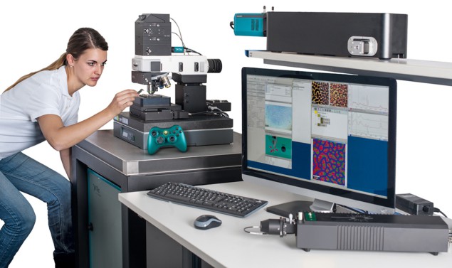
WITec’s modular design strategy gives users a clear upgrade path for their confocal Raman microscopy systems – as well as the opportunity to integrate with other microscopy techniques

WITec, a German manufacturer of nano-analytical microscope systems, is on a mission. Put simply, the Ulm-based vendor wants to democratize the use of confocal Raman microscopy across diverse research and industry applications spanning surface chemistry, solid-state physics, food science, environmental research, pharmaceuticals R&D and geosciences – and that’s just for starters.
This powerful diagnostic technique, which is fast losing its outsider status, provides label-free and non-destructive imaging (qualitative and quantitative) to map the chemical composition of heterogeneous samples at the submicron scale. What’s more, owing to the high confocality of WITec’s Raman microscopes, it’s possible to generate volume scans and 3D images using 2D image slices from a series of stepped focal planes.
Modular thinking
WITec’s immediate challenge, in terms of its product roadmap for confocal Raman microscopy, is to balance and prioritize user requirements that can sometimes appear contradictory: ease of use versus diverse functionality; optimized sensitivity across a range of applications; low cost plus leading-edge performance. With this in mind, WITec is pioneering a modular design strategy that gives users the ability to reconfigure their confocal Raman microscope across multiple unique research applications.
“We can optimize our systems for a range of requirements using specific combinations of optical building blocks – lasers, filters, lenses, spectrometers and detectors,” explains Olaf Hollricher, director of R&D and co-founder of WITec. “It’s a little bit like Lego in that users can upgrade and adapt the instrument as their research extends in new directions.”

For the customer, that clear upgrade path ultimately translates into cost savings, productivity gains and enhanced research outcomes. Equally significant, claims Hollricher, is the opportunity to combine confocal Raman microscopy with other microscopy techniques – for example, scanning electron microscopy (Raman-SEM) and atomic force microscopy (Raman-AFM).
The rationale is clear: by integrating different modalities into a single instrument platform, the user can build a more comprehensive picture of the sample under study. The Raman-AFM technique, for example, uses Raman imaging to obtain information about the type and distribution of molecules in a sample, while the AFM determines the surface characteristics. In this way, users are able to visualize chemical and morphological properties using a single instrument.
“The demand for these correlative microscopy techniques is growing among research and industry end-users,” says Hollricher. “Our customers recognize that they cannot get all the sample information they need using a single technique.”
The key to success is integration of complementary techniques into a unified, hybrid instrument design. “In order to correlate the data from these different approaches, it is essential to match and examine the same sample region in each case,” explains Hollricher. “If different instruments are used, finding and matching that sample region is a challenging and time-consuming exercise.”
Capabilities aside, the roll-out of these new correlative microscopy techniques is all about assimilation and education when it comes to the wider commercial opportunity. “After we introduced our Raman-SEM combination, it immediately triggered new sales,” says Hollricher. “However, you also have to be proactive and educate your current and prospective user base about the opportunities opened up by such innovations.”
Know your market
Right now, Hollricher and his WITec colleagues are focused on the final promotional push of the year at the Materials Research Society (MRS) Fall Meeting in Boston, Massachusetts (1–6 December). “You have to be present,” says Hollricher, pointing out that an international forum like MRS Fall is a great place to meet face-to-face with new and existing customers, R&D partners, as well as component and subsystem suppliers.
“After all,” he adds, “it’s much easier to do business if you know who you’re talking to and you’ve already met at a show like MRS Fall. These days, it’s also noticeable that prospective customers do their homework online before heading to a show, so their questions come from an informed perspective rather than a general fact-find.”
In anticipation of those questions, WITec will showcase a number of workflow innovations at MRS Fall. A case in point is TrueSurface, an optical correction technique that enables 3D chemical characterization of rough, inclined or irregularly shaped samples – including pharmaceutical coatings, composite emulsions and complex semiconductor structures – while retaining the strong rejection of out-of-focus light afforded by confocality.

Put simply, the TrueSurface module ensures the surface of large or coarsely textured samples remains in constant focus during a measurement. The sensor actively monitors and maintains a set distance between the objective and sample surface with submicron resolution. “This closed-loop operation can eliminate any temperature-induced focus drift during measurements with long integration times – for example, if you have to use a very low excitation intensity to measure overnight because your sample is sensitive,” Hollricher explains.
Also set to feature prominently on the WITec booth is ParticleScout, an analysis tool that enables researchers to find, classify, quantify and identify particle contaminants quickly and easily on a sample surface. ParticleScout employs a multistep process, beginning with a bright- and dark-field illumination survey of particle contaminants.
Image stitching then combines many measured regions into a large-area overview, while focus stacking allows larger particles to be sharply rendered for accurate outline recognition. Categorization of particles of interest into a ranked list is followed by automatic acquisition of a Raman spectrum for each particle, while the integrated TrueMatch Raman database software provides streamlined evaluation and identification.
“There are a growing number of applications where users need to analyse organic and microplastic particle contaminants,” notes Hollricher. “This is a hot topic for scientists in public water companies, breweries, bottled-water manufacturers, the food industry and in environmental agencies.”
Looking further ahead, Hollricher sees automation as the “next big thing” in confocal Raman microscopy. “Until recently, users needed a lot of expertise and domain knowledge to get the most out of Raman microscopy. What I see down the line is a move towards database-enabled search that yields valuable information and insights from a system that’s easy to operate for specialist and non-specialist users alike.”
- WITec will be exhibiting on booth 1008 at the MRS Fall Meeting (Boston, MA) from 1 to 6 December.
Figures of merit
Speed, sensitivity and resolution are three must-haves in a high-quality confocal Raman microscope – and they should not be mutually exclusive. The ideal Raman imaging system should therefore be configured such that high-resolution images with a high signal-to-noise ratio can be acquired in a short period of time.
Speed: In the past, exposure times from minutes to hours were common for acquiring a single Raman spectrum. Today, it takes just one second to record more than 1000 Raman spectra – i.e. a Raman image can be generated in a few minutes using optimized optics and an electron-multiplying CCD camera. Fast acquisition times are particularly important for measurements on sensitive and valuable samples in which the excitation energy must be kept as low as possible.
Sensitivity: A confocal beam path (i.e. using a diaphragm aperture) is essential for achieving the best possible sensitivity – eliminating light from outside the focal plane to increase the signal-to-noise ratio. The entire Raman imaging system should also be optimized for high light throughput. That means a spectrometer with a throughput in excess of 70%, designed for measurements with low light and low signal intensity. CCDs optimized for spectroscopy (greater than 90% quantum efficiency in the visible range) are most commonly used as detectors, while almost lossless photonic fibres ensure efficient light and signal transmission.
Resolution: Spatial resolution of a confocal Raman microscope is determined by the numerical aperture of the objective and the excitation wavelength – i.e. the smaller the aperture, the higher the spatial resolution. Lateral resolution is typically about 200–300 nm; depth resolution less than 1 micron. Spectral resolution defines the ability of a spectroscopic system to separate Raman lines adjacent to each other. A spectrometer design free of coma and astigmatism ensures symmetric spectral peaks, while the type of grating, focal length of the spectrometer, pixel size of the CCD camera and the aperture size all affect the spectral resolution. At room temperature, the width of the Raman lines is typically 3 cm–1, though some applications (low-temperature studies or stress analysis) may require significantly higher resolution.


