Silicon has been used to make electronic components and displays for over 30 years, but scientists have never fully understood how the element switches between its amorphous and crystalline forms during manufacture. Now Dimitrios Maroudas and colleagues at the University of California at Santa Barbara believe they have identified the key role that hydrogen plays in this transformation. The researchers hope that their discovery will streamline production processes and lead to cheaper silicon devices (S Sriraman et al 2002 Nature 418 62).
Amorphous and crystalline silicon have different electronic and optical properties, and this makes them suitable for different applications. Sheets of amorphous silicon are easier and cheaper to make than crystalline silicon, so this form is widely used for applications where large areas of silicon are needed, including displays and solar cells. In contrast, the smaller components used in devices such as computers are usually made of crystalline silicon, which can perform electronic operations more quickly.
Both types of silicon are made by depositing silicon from a plasma of ‘silane’ – that is, SiH4 – onto a substrate. This ‘plasma deposition’ technique is straightforward for amorphous silicon, but more complicated for crystalline silicon. And although scientists have long suspected that the hydrogen from the silane play an important role in this process, it has been unclear exactly how the two kinds of silicon are related.
Now Maroudas and colleagues have established that the hydrogen atoms can rearrange the atoms in amorphous silicon into the lattice structure found in crystalline silicon. The researchers proposed that the hydrogen atoms get trapped between loosely bound atoms in amorphous silicon to make a higher-energy Si-H-Si configuration. When the hydrogen atoms are later released, they proposed, the silicon atoms would be left in an ordered, crystalline array.
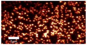
To test their theory, the Santa Barbara team ran a ‘molecular dynamics’ simulation to show how the deposition process would proceed if their idea were correct. They also deposited silicon from a silane plasma in which some of the hydrogen was replaced by deuterium. These ‘heavy hydrogen’ atoms can be distinguished from hydrogen atoms using infrared spectroscopy, so their motion can be monitored. When they compared scanning electron micrographs of the silicon deposits with the simulation, they found that the results were very similar, supporting their theory.
“This is a rare, if not the first, direct comparison of the structure of a ‘real’ film deposited in the laboratory with that of a ‘model’ film, which was made using computer simulations,” team member Eray Aydil told PhysicsWeb.
Maroudas and co-workers hope that their discovery will lead to a simpler and cheaper way of making crystalline silicon devices. They are also optimistic that it will shed light on the behaviour of other elements with covalent bonds similar to those in silicon.