“Atomically thin magnets were discovered barely two years ago and already form a vibrant field of research, which has shown a remarkable evolution in this short time,” says Patrick Maletinsky, principal investigator of the Quantum Sensing Lab at Basel University in Switzerland. Despite some groundbreaking results over the past few years, as Maletinsky points out, “Addressing nanoscale properties of these magnets remained an open challenge and one that only a few existing techniques could in principle address.” Among these techniques was “single-spin magnetometry”, a method he had developed for scanning probe experiments at Harvard University a few years previously. Alongside colleagues at the University of Basel, University of Geneva and École Polytechnique Fédérale de Lausanne (EPFL) in Switzerland, Maletinsky has now reported in Science experiments that establish the technique as “a unique tool to address nanoscale magnetism in van der Waals crystals, down to the limit of a single atomic layer”.
Key to the interest in 2D materials, as Maletinsky explains, is the ability to customize their properties by stacking layers of various 2D materials in different ways. For example, by twisting the angle between layers researchers have shown they can tune the properties of pristine bilayer graphene between opposing extremes from a Mott insulator to a superconductor, a discovery that Physics World awarded the Breakthrough of the year in 2018. When these stacked 2D materials are magnetic, Maletinsky describes the research as “experimentally uncharted territory”, rich with exciting proposals including predicted novel “spin textures” such as skyrmions.
The technological prospects are equally promising. “These are the thinnest possible magnets,” says Maletinsky. “They thus offer opportunities for miniaturization of devices, which no other approach or material can. In addition, the tunability yields new functionalities such as fully electrical manipulation and readout of magnetization, which is relevant for data storage.”
Researchers have used various approaches to study the magnetism in 2D materials, including measuring how the field from 2D materials affects the electronic transport properties, fluorescence and the magneto-optical Kerr effect. The advantage single-spin magnetometry offers over these approaches is that it can provide direct quantitative data with nanoscale resolution. “I would now consider single-spin magnetometry as a close-to-ideal tool to study the physics of atomically thin 2D magnets,” says Maletinsky.
Decorating diamonds
To measure the magnetism in their 2D samples Maletinsky and colleagues measured the spin levels of a nitrogen-vacancy (NV) defect in diamond, where a nitrogen atom substitutes a carbon atom in the crystal lattice next to a vacant crystal lattice site. The optical responses of NV defects, such as photoluminescence, have distinctive peaks in their spectra that result from the energy levels of the electron spin. Applying a magnetic field shifts the spin energy levels, a response described as the Zeeman effect. In the range of magnetic field values produced by samples of 2D magnets this shift is proportional to the field, providing a convenient, quantitative magnetometer.
“The technique we employ – DC [direct current] NV magnetometry – is conceptually rather straightforward and mastered by many labs worldwide,” says Maletinsky. “The real difficulty comes about when one wants to perform nanoscale magnetic imaging using scanning NV centres and this approach is required to achieve the results we report on in our paper.”
Our solution for this are advanced all-diamond scanning probes
He highlights how important it was to have access to high quality samples, and his good fortune to collaborate with the group of Alberto Morpurgo at the University of Geneva who had mastered the non-trivial task of preparing excellent samples in a robust and controlled way. In addition, he describes two difficulties nanoscale studies raise: combining scanning probe microscopy (SPM) with an approach that allows efficient measurement of optical responses of the NV spins; and a robust method to add an NV centre to the tip of the SPM probe.
“I would consider this last part as the key crux for our experiments,” he adds. “Our solution for this are advanced all-diamond scanning probes, which we fabricate with my group in Basel and whose first generation I originally developed while still a postdoc in the lab of Amir Yacoby in Harvard.” The result is a technique that can quantitatively determine key magnetic properties of 2D crystals and directly image magnetic domains with spatial resolutions of just a few tens of nanometres.
Lucky break
Maletinsky says that a back of the envelope calculation was enough to suggest that their approach should work. So although experiments do not always go to plan the successful imaging was not a total surprise. However, the study was not without its white-knuckle moments, and one in particular proved to be a blessing in disguise.

“About halfway through our planned measurement campaign, my student Lucas Thiel, who is the main author of the paper, came to my office all depressed to report to me that he had destroyed one of our precious samples by an operator error in our setup (SPMs are not very forgiving in this regard) and that none of the data he took after this crash made any sense to him anymore,” says Maletinsky. “This was especially problematic since we had already acquired a rather extensive dataset on the sample in question and its loss would have meant a setback of several weeks.”
It took us several weeks to convince ourselves that this accident had indeed been a very fortunate event
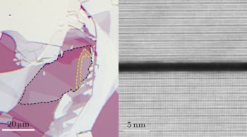
After initially mourning the accident, Maletinsky says they went back and analysed the post-crash data in more detail and found that what had initially made no sense, in fact explained an effect that had long puzzled researchers studying CrI3. In the bulk CrI3 is ferromagnetic, that is, all the spins align to give strong magnetic properties that are stronger for larger samples. In contrast studies of samples of few-layer 2D CrI3 all have either zero magnetism or the same magnetism as a monolayer, suggesting that the spins of adjacent layers are antiparallel. However, the magnetism of the punctured sample was roughly nine times the magnetism of a monolayer. Crucially the punctured sample was also nine layers thick, prompting the researchers to compare Raman measurements of the damaged sample with a pristine flake to determine whether there were differences in the crystalline structure.
Diamond quantum sensor breaks new record
“Even though the story and explanation might appear obvious in hindsight, it took us several weeks with additional control experiments and extensive discussions with our collaborators from Geneva to convince ourselves that this accident had indeed been a very fortunate event,” says Maletinsky. “In fact, it had offered us an explanation for one of the bigger questions in the field, namely why CrI3 showed the puzzling “even-odd effect” that we could now clearly link to a structural distortion in the material and one that we could “undo” using our puncture.”
NV-magnetometry for all
- So will this become the go-to tool for 2D magnet experiments worldwide? Unfortunately the availability of the all-diamond NV decorated tips Maletinsky and collaborators used remains a key obstacle as so few groups worldwide fabricate and employ them: Maletinsky’s group at Basel University, Yacoby’s group at Harvard and the group at University of California at Santa Barbara run by Ania Bleszinsky Jayich. The group run by Christian Degen at ETH Zürich also designs, builds and operates scanning probe microscopes that incorporate NV centers at the tip apex.
“Given my strong belief that this technique could be broadly applicable and useful to various areas of science, we recently spun out the startup company Qnami to overcome this shortcoming,” Maletinsky tells Physics World. “Qnami’s mission is thereby to provide commercial solutions for scanning NV magnetometry and in particular our hard-to-fabricate diamond tips.” Qnami already sells tips to research groups including those run by Jörg Wrachtrup at Stuttgart University in Germany and Vincent Jacques at Montpellier University in France and will reach out to first beta testers for a complete magnetometer-based quantum microscope later this year.
- This article was updated 2 May 2019 to include the Degen Lab among those using diamond NV decorated tips.