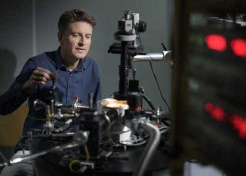
A team of researchers at the University of Twente in the Netherlands has employed deep learning – a form of artificial intelligence, or AI – to optimize the structure of nanoelectronics devices for the first time. According to team leader Wilfred Van der Wiel, the same method could also be used to tune quantum dot systems for quantum computing and should be generally applicable to other large-scale physical systems for which many control parameters are likewise unavailable.
Earlier in 2020 Van der Wiel and colleagues created an electrically tuneable network of boron dopants in silicon. This device contained eight terminals, or electrodes: seven that act as voltage inputs and one that serves as a current output. The signal of the output comes from electrons “hopping” from one boron atom to another in a way that somewhat resembles the way neurons in our brain “fire” when they perform a task. So, while the network is not ordered, it has an output signal, and it is possible to “steer” this signal in the desired direction by changing the voltages on the control electrodes.
This process is also called artificial evolution, Van der Wiel explains, and although successful it proved cumbersome in practice. “While not as slow as Darwinian evolution, it is still quite time-consuming to have the network do what you would like it to do,” he tells Physics World.
Making use of deep-learning neural networks
For this latest work, the Twente team turned instead to deep neural networks (DNNs). These networks have become increasingly common tools in scientific research, where they are typically used to model complex physical phenomena after an initial period of “training” on examples drawn from experimental data.
To generate a DNN model of their nanoelectronic device, Van der Wiel and colleagues began by measuring the device’s output signal for many distinct input voltage configurations. They then used these data and standard deep-learning techniques to train their DNN model to “understand” how the real device behaves. The resulting model predicts the output current of the device, given the input voltage configuration. Van de Wiel explains that this approach is very similar to the way that standard AI tasks are solved using DNN. “In standard deep learning, we have to find the parameters of the model itself,” he says. “These are the weight factors between neurons and the threshold values of the neurons. This is what we learn in the first phase: we find the parameters of the DNN model itself, so that it mimics the physical device.”
100 times faster than artificial evolution technique
In the second phase of their work, the researchers keep the parameters of the DNN model constant so that they can learn the optimum control parameters. “With this model, we can search for a desired functionality,” Van der Wiel says. “For this, we choose some of the inputs as control parameters and others as data inputs. We search for the control values on the DNN model again using deep learning. Mathematically this boils down to the same thing: again, we have to optimize parameters to find the desired output.”
Once they have used the DNN to find the best values for the control parameters, the researchers can apply these values as voltages to the corresponding terminals in the real nanoelectronic device. Since the DNN is a model of the physical device, its output current should then behave in the desired way.
The group found that this new approach works about 100 times faster than the artificial evolution they used before. “With this new method we can optimize nanoelectronics devices with many terminals and even optimize systems in which many complex nanoelectronics circuits are coupled,” Van der Wiel explains. “Such systems are expected to increase in complexity in the coming years in, for example, novel information processing technologies like quantum computing and neuromorphic computing.”
Scalable and applicable to complex tasks
Van der Wiel and colleagues also found that their approach worked for tasks of increasing complexity. After successfully demonstrating Boolean gates on their nanoelectronics device, they went on to show that the device can perform binary classification and a “feature map” task in which 2 × 2 patches of pixels are mapped to a current value (a subtask of a higher-level image classification task). These last two tasks would have been very challenging to complete without this new method, the researchers say.
Neural networks, explained

The dopant network devices described in this study, which is published in Nature Nanotechnology, could be used for neuromorphic computing in the future. As a next step, the team plans to build more energy-efficient large-scale systems of interconnected dopant network devices for state-of-the-art AI performance.