Like many 2D materials, gallium sports some fascinating properties when in the form of atom thick layers. It has a superconducting transition temperature at 5.4 K and interesting superconductor-metal transitions with increasing magnetic field. In addition, like bulk gallium, which is widely used in electronics in III-V semiconductor compounds, 2D gallenene may also be useful in optoelectronic devices. In a recent 2D Materials report, Jun-Zhong Wang and colleagues at the School of Physical Science and Technology Southwest University in China show how to grow gallenene epitaxially on the (1 1 1) plane of silicon, helping towards the possible incorporation of gallenene in future electronic and optoelectronic devices.
Despite the success of epitaxial growth to produce graphene and other 2D materials, with its low melting temperature growing 2D gallium has presented difficulties. As Wang and colleagues point out the 7 × 7 (1 1 1) plane of silicon – the crystal orientation of the wafers commonly used for silicon electronics – has dangling bonds that interact strongly with gallium atoms and inhibit their migration along the surface.
Previous work by researchers at Rice University and Hysitron Inc in the US reported gallenene production by exfoliating from molten gallium but Wang and colleagues have shown that it is possible to epitaxially grow gallenene on silicon.
Layered success
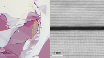
The researchers deposit a third of a monolayer of gallium on the Si(1 1 1) − 7 × 7 surface at room temperature and anneal it at 550 °C for 30 min to produce a layer of √3 × √3 gallium. They then grow a buffer layer at 50 °C using a beam of gallium at a flux of 0.2 monolayers per minute. On this buffer layer they could readily grow honeycomb 2D gallanene.
They use scanning tunnelling microscopy alongside first principal calculations to derive the structure of the layers, identifying a 4 × √13 structure for the buffer layer. They also confirm the metallic behaviour of the gallenene top layer.
“As we all know, silicon is the backbone of the traditional semiconductor industry,” explain Wang and colleagues in their report. “If gallenene can be synthesized on the surface of silicon, its potential applications in optoelectronic and microelectronic devices will be greatly improved.”
Full details are reported in 2018 2D Materials 5 035009