New materials are often the driving force behind technological breakthroughs. Hannah Stern tells Katherine Skipper why she’s developing new platforms for encoding, transmitting and manipulating quantum information

Every year one early-career researcher who’s made “exceptional contributions to experimental physics” is awarded the Henry Moseley medal and prize from the Institute of Physics (IOP). In 2023 the medal was given to Hannah Stern for her work on understanding the photophysics of semiconductors and 2D materials. As of January, Stern is an assistant professor at the Photon Science Institute at the University of Manchester, UK. She was previously a research fellow at the University of Cambridge, where she also obtained her PhD in 2017.
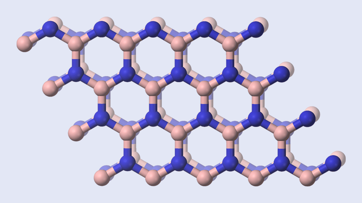
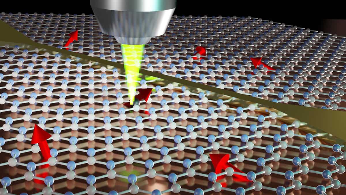
Stern’s group is developing new platforms for quantum technologies, with a focus on materials with quantum states that can be controlled with light. She recently led research with colleagues in the UK and Australia which showed that lattice point defects in hexagonal boron nitride (hBN) have promising properties for quantum technologies, including sensing and optical networking (Nature Materials 10.1038/s41563-024-01887-z).
Katherine Skipper caught up with Stern to discover what motivates her research, what the big challenges facing the quantum sector are, and what the ethos of her new group will be.
What first sparked your interest in quantum technology?
I’ve always been intrigued by quantum mechanics. When I was an undergraduate at Otago University in New Zealand, I majored in physical chemistry, and I gained experience with spectroscopic techniques. In these experiments, we would shine light at materials and use the data we collected to understand the electronic structure of those materials on the atomic and molecular level. I found this exciting because it felt like I could really see quantum mechanics at work.
I continued with different forms of spectroscopy for my PhD and learnt a lot more about electronic spin states in materials that could be generated via light. I didn’t start thinking about the implications of these systems for quantum technologies until later. As a postdoc, I became interested in states in materials that emit single photons at a time. That was when I realized that the physics I had been studying had applications within quantum technology.
Your research is on light–matter interfaces for quantum technologies. Why is the interaction between light and matter important for quantum applications?
Understanding the interaction between light and matter has always been central to building our understanding of quantum mechanics. Today, light–matter interactions on the single particle level are one of the most useful ways to control and use quantum phenomena for new technologies.
In the first instance, quantum technologies require qubits, which are the quantum equivalent of the classical bit. In simple terms, a qubit is a two-level system that can exist in a quantum superposition state. Qubits can be formed not only from electronic and magnetic transitions within materials but also from single photons. Both form of qubits are being actively developed for different applications.
While light and matter qubits can be used separately for quantum technologies, we can get new functionality by harnessing the interaction between them
For example, photons are useful for applications that require transportation of quantum states (i.e. for communication technologies) because they can be sent long distances without losing quantum information, which may be encoded in the photon polarization, for example. Qubits in matter, however, such as electronic or nuclear spins, are often better at storing information for longer periods of time. Typically, they can also be controlled more easily than photons so they are more suitable for performing logical operations on the device level, for example in computing or simulation.
The dream of a ‘quantum internet’ is closer than you might think
What this means is that while light and matter qubits can be used separately for quantum technologies, we can get new functionality by harnessing the interaction between them. A good example is “quantum optical networks”. Long-distance optical quantum networks don’t exist yet, but it could enable a quantum version of the internet, in which quantum information is distributed across a series of globally positioned nodes.
These nodes could be material qubits, which would send and receive quantum information from photons and store it locally as a quantum memory. As it turns out, a promising material system for this is atomic-scale point defects in materials, which is what I work on.
What kind of qubits in matter do you study? And how does the interaction with light enable these systems?
Qubits in matter often come in the form of electronic or nuclear spin transitions of atoms or molecules – what are called “spin qubits”. Spin is one of the non-intuitive concepts of quantum mechanics that doesn’t have a classical analogue – it refers to an intrinsic property (angular momentum) of a particle. Importantly, spin is quantized, meaning particles can only exist in a limited number of possible spin states.
What’s interesting about the spin qubits I work with is that the state of the qubit can be controlled with light
The simplest example is the spin state of a single electron, which can be spin up, spin down or a superposition of those two states. Often the spin state of an atom, defect or molecule is slightly more complex – in fact, the materials I work with are an example of this. But it’s typically still possible to think about the spin state in this way.
What’s interesting about the spin qubits I work with is that the state of the qubit can be controlled with light. We first use a laser pulse to place the qubit into a useful spin state before manipulating it with a second electromagnetic pulse and using a second laser pulse to “read-out” the new state. Known as optically detected magnetic resonance, it forms the basis of how we use the spin qubit to store quantum information or sense the environment.
The systems I work with are formed from atomic-scale point defects in an extended solid, in this case a 2D material. You could think of these defects as a missing atom in the lattice. The disruption of the lattice creates a “trapped molecule” in the crystal, which is electronically isolated and has well defined electronic transitions between optical and spin states, forming a qubit.
One appealing feature of defects in solids for quantum applications is that they work at ambient conditions, without needing low temperatures or high magnetic fields. The spin control pulse in our experiments is generally in the microwave or radio range, which is good because we can easily implement microwave or radio frequency control on a chip, and at room temperature. It’s quite hard to find other isolated quantum objects that can be manipulated at ambient conditions.
What are the applications of spin qubits?
In addition to optical networking applications, one important application is in sensing. Most sensors measure a physical quantity over a bulk, or spatially averaged, sample. An exciting feature of sensors based on single electronic spins is that the sensor itself is now atomic scale and can measure physical quantities with very high (near atomic-scale) spatial resolution.
One particularly active area of quantum sensing right now is quantum nanoscale magnetometry
One particularly active area of quantum sensing right now is quantum nanoscale magnetometry, which exploits the fact that an external magnetic field will shift the energy of the electronic spin states of a spin qubit.
By measuring the energy shift of the spin states (via optically detected magnetic resonance), we can work out the magnitude and direction of the field at a precise point in space. So by scanning the qubit over a sample, the nanoscale magnetism of materials can be visualized in a way that has not been possible before.
What kinds of materials have spin properties that can be used in quantum technologies?
Several factors determine if a material will be useful for quantum technologies, and they also depend on the technology you are talking about. Typically, if a material that hosts spin qubits is going to be useful for a quantum application, it needs to have a significant spin coherence time, which is how long a spin can hold on to quantum information.
For sensing, generally the longer the coherence time the more sensitive the sensor. For optical networking, the spin coherence time limits how far the photon can be sent in the network. For both applications, typically a coherence time of at least milliseconds is desirable.
The coherence time of a spin qubit can be limited by a range of environmental factors. For solid-state spin qubits based on defects, the most common limitation is magnetic noise from neighbouring nuclear spins and electronic impurities. This means that the spin needs to be isolated, so we typically use materials with a low abundance of spin-active nuclei. Diamond is well known for this.
You’ve recently investigated the spin properties of defects in hBN: what makes it attractive for quantum applications?
hBN is a 2D material with a wide band gap. Because it’s an insulator, we wouldn’t expect it to interact with visible wavelengths of light, but in about 2016 localized emission of visible light was observed in a hBN lattice (Nature Nanotechnology 11 37).
The idea was put forward that this emission comes from atomic-scale defects in the lattice. By the time I got interested, quite a lot of work had been done to optically characterize the defects, but we didn’t know whether this optical transition could interact with an electronic spin state of the defect.

At that point, there was the nitrogen-vacancy centre in diamond and a couple of other defects in silicon carbide, but not many other defects in materials that offered optically addressable electronic spin qubits.
In our most recent paper, we’ve shown that there are spin states of these defects that we can initialize, control and then read out using light. And these defects can store quantum information for microseconds at room temperature.
Graphene at 20: why the ‘wonder material’ is finally coming good
In addition, many spin qubits require a magnetic field to operate, either to initialize the qubit or to separate the spin qubit transitions from other electronic transitions. Here however, we can control the spin without any magnetic field. While the coherence times are still relatively short compared to other systems, this is all being performed under ambient conditions and in a brand new material platform.
This is also the first time spin defects with these properties have been studied in a layered material as opposed to a bulk crystal. 2D materials offer natural advantages for fabrication because they can be easily moved from surface to surface and incorporated with other materials and optical components, such as wave guides or cavities, that we may like to use in future to improve the collection of light from the defects. It can be extremely challenging to couple photons coming from the middle of a crystal to such components.
All of these things are quite exciting because they speak to this type of physics being available in a device that might operate in real world conditions.
What further work is needed to take hBN out of the lab and into real-world devices?
We have a lot to do. We’re interested in technologies that use both the spins and the photons of the hBN defects, and while we’ve made some strides in understanding the spin physics, we’ve got a lot more to understand on the optical properties. A big challenge before us is identifying the chemical structure of the defect. We believe it’s related to carbon inserted in the lattice but we don’t know the exact arrangement of the carbon atoms in the hBN lattice and that’s what we’re working hard to determine in collaboration with theorists.

The next thing will also be to control the growth of the hBN better and we’re working with collaborators on that. We want to create a defect exactly where we want it in the 2D material. This is a massive challenge but we’re hopeful that the 2D material will enable this.
Further work will also involve working with companies who are interested in this space, eventually moving towards implementing this material in a full device.
The quantum sector has been growing rapidly but what are the biggest challenges in commercializing the technology?
We are at a point now as a community where a lot has been demonstrated in laboratories and many of the existing challenges are about scaling. For quantum computation with solid-state spins, this means scaling to more and more qubits, while for optical networking, it’s about scaling to more and more nodes.
To achieve scalability, we need to interface different materials with each other and interface quantum systems with classical electronics and optical components
There are also challenges related to materials development. To achieve scalability, we need to interface different materials with each other and interface quantum systems with classical electronics and optical components. One part of achieving this that I’m particularly interested in is identifying new quantum systems in new materials that offer advantages or alternative possibilities alongside the existing ones.
We’re seeing that this is an exciting new direction in the field – to look at other material systems and explore these to build a broader material toolkit.
You’ve recently set up your own group in Manchester. What do you want its ethos to be?
The group is multidisciplinary and interdisciplinary and I think that’s important. We cover physics, chemistry, materials science and electronic engineering. Having a lot of different views in the room and scientific backgrounds encourages creativity, and it also contributes to scientific risk-taking. In some respects, the work on defects in hBN was risk-taking at the beginning because we didn’t know what we would find.
I’m also hoping to build a group where anyone from any background, nationality or minority is welcome. I think it’s important the group be broadly inclusive and representative of society. I’ll work hard to make sure it stays that way.


