Nitrogen-vacancy (NV) impurities in nanodiamonds could be used as single-photon sources in quantum technologies, such as quantum computers and quantum sensors, thanks to their unique optical and electronic properties. However, the problem is that their emission spectra contain unwanted broad emission bands in the red part of the electromagnetic spectrum. These are known as phonon sideband emissions and they need to be suppressed if real-world applications based on these defects are to see the light of day. A team of researchers in the Department of Physics at the Indian Institute of Technology (IIT) Ropar in India is now reporting on a new way to suppress these emissions in nanodiamonds using photonic crystals. Their technique, which works at room temperature, also enhances zero phonon line intensity in these materials as a further improvement.
Quantum information technologies will require stable quantum light emitters that can emit single photons at room temperature, explain Sachin Sharma and Rajesh V. Nair, who are from the Laboratory for Nano-scale Optics and Meta-materials (LaNOM) at IIT Ropar. In recent years, solid-state emitters, such as the colour centres in diamond have emerged as good candidates for such emitters because they are photostable and have a high quantum efficiency at room temperature.
The NV centre is one of the hundreds of colour centres found in natural diamond. These colour centres are atomic impurities and give rise to the pink, blue and yellow hues often seen in the precious stones. The NV centre involves two adjacent carbon atoms in the diamond lattice being replaced by a nitrogen atom and an empty lattice site (or vacancy).
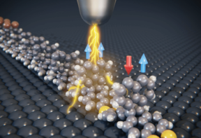
When illuminated with laser light of a certain colour, the NV centre emits light of another colour and the wavelength of this light depends on the charge state of the NV. Another important property of the NV centre is its good coherence, that is, its spin is shielded from the surrounding environment. This is why it can be used to store and process quantum information.
Two charge states
The NV centre mostly exists in two charge states, namely the neutral NV centre (NV0) and negative NV centre (NV–), explain Sharma and Nair. The NV– is particularly interesting because it has optically addressable spin states, which makes it more suitable for applications like high-resolution magnetometry, nanoscale thermometry and quantum information processing.
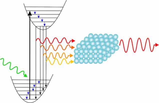
The NV centre emission spectra contain peaks at 575 nm and 637 nm. These correspond to the so-called zero phonon lines (ZPLs) of NV0 and NV– centres respectively. These peaks are accompanied by broad light emission bands on the red side called phonon sidebands (PSBs), which limit the use of the NV centre as a single-photon source at room temperature, explains Nair. “These phonon sidebands are in fact non-resonant transitions in the crystal lattice that cause decoherence in the system and hence need to be suppressed. But, to reduce decoherence completely, we also need to enhance the ZPL intensity as well as suppressing the PSBs.”
Making use of photonic “stop gaps”
The researchers say they have now developed a simple but efficient way to do both of these things at room temperature. “For supressing the PSBs, we made use of photonic ‘stop gaps’ of photonic crystals with closely spaced lattice constants to cover the broad spectral range of PSB emission,” says Nair. “The multiple stop gaps cover most of this emission.”
Photonic crystals are nanostructured materials in which a periodic variation of the refractive index on the length scale of visible light produces a photonic “band gap”. This gap affects how photons propagate through the material and is similar to the way in which a periodic potential in semiconductors affects the flow of electrons by defining allowed and forbidden energy bands. In the case of photonic crystals, light of certain wavelength ranges can pass through the photonic band gap while light in other ranges is reflected.
Photonic band gaps form thanks to the interplay between two resonance light scattering mechanisms. It is one of these, the macroscopic Bragg resonance (which is the resonance from a periodic array of light scatterers in a material) that is responsible for producing photonic stop gaps. These form an exponentially decaying wave in the direction of the periodic variation of the refractive index when an integer number of half wavelengths coincides with the lattice spacing of the photonic crystal itself.
Enhancing the ZPL intensity too
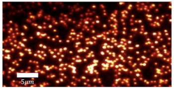
In their experiments, which they report in Optics Letters, Sharma and Nair used commercial nanodiamonds that are around 70 nm in size and which contain more than 300 NVs. “We thus considered an ensemble of emitters rather than a single one,” they explain, “and synthesized our photonic crystals using polystyrene spheres with diameters of 196 nm, 287 nm and 295 nm in a technique called colloidal self-assembly.” The researchers used the 196-nm-sized sample as their “reference” since its stop gap (of 445 nm) is centred far away from the NV centre emission spectra, which makes it easier to study.
And as a plus, they also succeeded in increasing the ZPL intensity by precisely tuning the photonic band edge of the photonic crystal to the ZPL wavelength. ZPLs are pure electronic transitions that do not involve lattice phonons, so enhancing these means that there is no decoherence in the system, says Nair.
“Our work could open the way to studying the NV centre in more detail for quantum nanophotonics and biophotonics applications,” he tells Physics World. “It might even help, for example, in the development of advanced technologies such as NV-centre-based lasers operating at ZPLs.”


