Nanostructuring a thin layer of the semiconductor germanium using a technique called nanoimprinting lithography can greatly boost the amount of light it absorbs across the visible to near-infrared wavelengths. The broadband absorption comes from the strong interplay between Brewster and photonic crystal modes in the material and the effect could benefit optoelectronics applications such as photovoltaics and telecommunications.
Designing ultrathin semiconducting materials that absorb light over a broad range of wavelengths is crucial for making improved optoelectronics devices that more efficiently convert light into active electrons. One way of achieving this is to increase the thickness of the semiconductor layer so that it can capture the maximum number of photons across the optical spectrum.
Researchers at the Institut de Ciència de Materials de Barcelona in Spain have taken a different approach to this one by employing different light-trapping strategies so that a reduced amount of semiconductor is still able to strongly absorb light. In the photonic metastructure they studied, incoming light is coupled to different types of light resonant modes: Brewster and hybrid photonic-plasmonic resonant modes. It is these resonances that are responsible for concentrating the light electric field in small volumes and so allow the material to absorb light over the visible to the NIR range (400–1500–nm).
Two effective thicknesses of germanium for light to interact with
A Brewster mode is a photonic mode in which there is no light reflected from the surface, explains team leader Agustin Mihi. “A thin layer of semiconductor, like the one we used in our study, on a noble metal substrate sustains this type of mode thanks to the high refractive index of the semiconductor and the non-ideal behaviour of noble metals in the visible part of the optical spectrum. In this mode, light is strongly confined in the thin film at wavelengths determined by its thickness.
“Because of the nanostructuring of the germanium (Ge) film in our sample, there are two effective thicknesses of Ge that light can interact with: the thinner one with the Brewster mode and the thicker one with the plasmonic-photonic mode.”
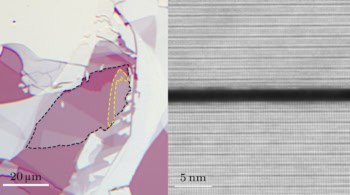
The metastructure made by the researchers comprises a Ge 2D square array of cylindrical holes built on top of a gold film using soft lithography – a scalable technique that has the advantage of being compatible with mass production processes such as roll to roll.
Metasurface exhibits a series of photonic resonances
“It is challenging to achieve broadband light absorption through photonic resonances alone because each resonance amplifying light absorption acts only over a specific wavelength range,” says Mihi. “In our experiments, we make a metasurface that exhibits a series of photonic resonances from the NIR to the visible, increasing the light absorption of the Ge layer at all energies above its electronic bandgap.”
The broadband absorption in fact comes from the simultaneous excitation of the different resonances throughout the entire absorption spectra of the Ge layer, he tells nanotechweb.org. “In the visible, our photonic architecture sustains a broad Fabry Perot resonance, which is enhanced by coupling with a Brewster mode, as mentioned. In the NIR, there are multiple absorption peaks coming from the plasmonic-photonic modes excited in the photonic crystal fabricated on top of the metal substrate.
Applications in photovoltaics and telecommunications
“The photonic crystal provides ways to couple the light in the in-plane direction of the ultrathin Ge film, allowing it to confine long wavelength photons (up to 1400 nm),” he adds. “We also carefully design the metasurface to couple this light to slow light modes, which combine photonic crystal and plasmonic effects, resulting in strong absorption peaks.”
Such strong broadband absorption could be useful for making more efficient photovoltaics devices and the NIR absorption in particular (which reaches 100% over the important telecommunications window) could benefit applications such as photodetectors, he says.
The team, reporting its work in Advanced Materials DOI: 10.1002/adma.201705876, is now busy designing different optoelectronics devices using its nanostructured Ge. “These include third-generation solar cells (based on perovskite materials). We hope to improve their efficiency and make them competitive with established silicon technology.”