Using the electric field of a scanning tunnelling microscope (STM), scientists in the US, Europe and Japan have created nanoscale circular p-n junctions in graphene. By controlling the voltage between the probe tip and the substrate, the researchers altered the size of the junction, forming deep, narrow electron traps, or broad optical wave guides. The work overcomes one of the main challenges in exploiting graphene’s unique electronic structure, and could be used to create all-in-one, multifunctional optoelectronic devices with unprecedented capabilities.
p–n junctions are formed at the interface between two materials, or between differently doped regions of the same material. The positive, p-doped side corresponds to an excess of holes, and the negative, n-doped side an excess of electrons. Individually, both sides of the junction are good conductors, but when brought together an external bias is required for a current to flow. By reversing this bias, the flow can be stopped. This principle underlies the binary “on/off” states on which digital logic commands are built.
One of the fundamental difficulties in using such structures in graphene-based electronics arises from the linear (Dirac-like) energy dispersion of the material’s electrons. This means that electrons can travel through potential barriers of infinite height, making the “off” state very hard to achieve. Now, Eva Andrei at Rutgers University in the US, and colleagues in the US, Belgium and Japan, have found a way to bring these electrons under control.
Andrei and her team created nanoscale circular p–n junctions using the electric field of a nearby STM tip. Positively biasing the tip attracts negative charges to a circular region in the graphene directly below. The interface between this n-doped region and the p-doped graphene around it forms the p–n junction.
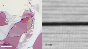
Doping levels in each of these regions can be tuned easily by changing the voltage applied to the tip or the substrate. The size of the junction can be controlled to some extent by the doping, but producing a junction of the smallest lateral extent requires an atomically sharp STM tip. The researchers achieved this by pressing the probe tip repeatedly into gold before slowly retracting it. Each iteration caused gold atoms to be dragged out at the apex of the tip, eventually forming a narrow gold nanorod on the end.
The team discovered that when the circular junctions are very small, they act as deep, narrow potential wells that trap the graphene’s Dirac electrons. When a smaller voltage is applied to the underlying silicon, the potential well becomes broader and can no longer trap electrons. Instead it becomes host to a set of electronic modes that can be used as optical guides.
Creating these junctions near a reflecting plane – a gold contact in this case – can enhance their optical guiding capabilities. Electronic modes from the junction travel outwards like ripples in a pond and reflect from the contact. They form a standing wave pattern that spans an area much larger than the lone p–n junction.
The p–n junctions created by Andrei and colleagues provide a mechanism to confine electrons in graphene and, with simple tuning, can act as optical guides, providing a bridge between electronics and optics. Now that the dynamics of p–n junction formation have been described, more sophisticated architectures can be achieved by depositing nanowire or nanodot arrays on gated graphene samples, avoiding the complexity and cost of using an STM probe. The technique promises unique and interesting future applications.
Full details of the research are reported in Nature Nanotechnology.