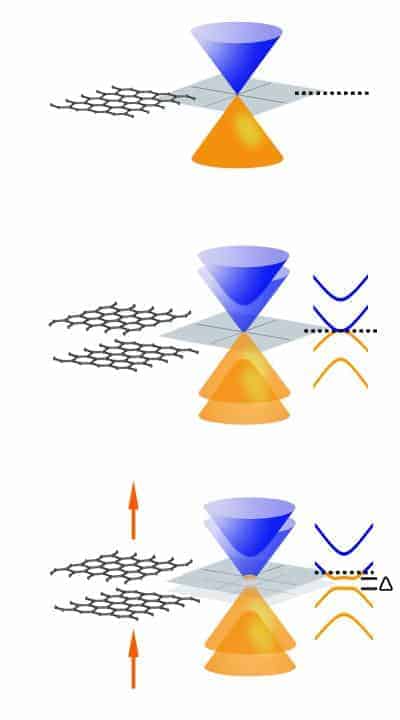
Researchers in the US have the best evidence yet that the electronic band gap in bilayer graphene can be adjusted by changing an applied voltage. This is unlike conventional semiconductors such as silicon in which the gap is fixed by the material’s crystal structure and chemical composition. The band gap is of great importance when designing semiconductor devices and the ability to adjust its value could make graphene a promising material for future electronic and optical devices.
Graphene is a sheet of carbon just one atom thick and is normally a metal capable of conducting electrons at extremely high speeds — the electrons behave like relativistic particles that have no rest mass. However, under certain conditions it also behaves like a semiconductor and these and other unusual physical properties, means that graphene is often touted to replace silicon as the electronic material of choice in the future.
The electronic band gap is the energy difference between the valence and conduction bands in a semiconductor or metal — and its existence is what allows semiconductor devices to switch electrical currents on and off.
Dialling up light
A semiconductor with a “tuneable” gap that can be changed externally –- by applying a voltage, for example –- could lead to new types of electronic devices, notably lasers where the wavelength of the light could be dialled-up with great precision.
Graphene normally has a band gap of zero, which is related to its massless electrons. In 2007, a team of physicists showed that the electrons in bilayer graphene — a sheet of carbon two atoms thick — appeared to acquire mass when a small external voltage was applied across the sheet. This, they said, is proof that an energy gap could be created and controlled.
Now Feng Wang and colleagues at the University of California at Berkeley have made a more direct mesurement of the band gap in bilayer graphene as the external voltage is varied from 0 to 250 mV at room temperature.
The narrow bandgap range means that it could now be possible to make new types of nanotransistors, nano-LEDs and other nano-optical devices in the infrared range from graphene.
Field-effect transistor
The team made a two-gated bilayer device from graphene. The device, which is a field-effect transistor, is built on a silicon substrate (the bottom gate) and contains a thin insulating layer of silicon dioxide between the substrate and the graphene layers. There is a transparent layer of sapphire (aluminium oxide) over the graphene layers and on top of this, the top gate, made of platinum.
The researchers varied the applied voltage to the gate electrodes and measured how the bandgap changed. They did this by sending an infrared beam (from the Advanced Light Source facility at the Lawrence Berkeley National Lab) into the device and measuring variations in the amount of light absorbed by the graphene layers. The size of the absorption peak in each spectrum gives the exact size of the bandgap at each gate voltage.
The team is now trying to improve the bilayer device for use in high-performance tunable electronics. “We will also try to understand the light emission behaviour from such a tunable semiconductor,” Wang said.
The work was published in Nature.


