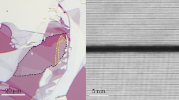
Researchers in China and Korea have grown large-scale single-crystal monolayers of a two-dimensional material, tungsten disulphide (WS2), for the first time. The crystals, which were grown on a sapphire substrate, measured more than 3 cm across, and could become an alternative platform to silicon in next-generation semiconductor technology.
Silicon-based semiconductors are fast approaching their performance limits, so researchers are seeking new materials to replace them. Two-dimensional materials such as graphene (the most famous of all 2D materials) and WS2 show great promise in this context. The latter belongs to a family of materials known as transition metal dichalcogenides (TMDs), all of which have the chemical formula MX2 (where M is a transition metal such as tungsten or molybdenum and X is a chalcogen such as sulphur, selenium or tellurium).
The TMDs have a special property. While they are indirect band-gap semiconductors in their bulk form, they become direct band-gap semiconductors when scaled down to monolayer thickness. These monolayers efficiently absorb and emit light, and so might find use in optoelectronics devices such as light-emitting diodes, lasers, photodetectors or solar cells. They might also be used to make circuits for low-power electronics, low-cost or flexible displays, sensors and even flexible electronics that can be coated onto a variety of surfaces.
Difficult to grow as single-crystal structures
The problem is that it has so far proved difficult to grow TMDs as single-crystal structures on insulating wafer-scale substrates – the sine qua non for building ultra-large-scale high-performance semiconducting circuits. This is because the crystalline lattice of TMDS is not symmetrical, which generally leads to islands of the material being aligned antiparallel on most substrate surfaces.
Two teams, led by Kaihui Liu of China’s Peking University and by Feng Ding from the Center for Multidimensional Carbon Materials at the Institute for Basic Science (IBS) in Korea, together with collaborators at Fudan University, have now overcome this problem. Inspired by crystal growth techniques that involve aligned nanotubes on sapphire, Liu, Ding and colleagues grew their WS2 on a single-crystal sapphire substrate cut along a specific plane at an angle of just 0.1°. This sapphire structure is known as vicinal a-plane sapphire (or a-Al2O3). The method, which the researchers call “dual-coupling guided epitaxy growth”, favours a coupling between WS2 and the edges of the sapphire that breaks the antiparallel orientations of the WS2 islands on the substrate. All the TMD single crystals grown on the substrate are thus aligned along a single direction. These small single crystals then coalesce, producing a larger single crystal that matches the dimensions of the substrate.
‘Most perfect graphene ever’ grows fold-free on metal foil
By showing that it is possible to grow wafer-scale 2D single crystals other than graphene, and on insulating surfaces other than the more common hexagonal boron nitride, the researchers say they have taken a major step forward in 2D-materials-based device design – one that could aid the development of 2D semiconductors in high-end applications of electronic and optical devices. Looking ahead, members of the team are now busy developing next-generation technology and theories for how to synthesize a broad class of 2D materials in wafer-scale single-crystal form. “We will be making a great effort to improve the quality of the synthesized 2D materials and even control their thickness in the future,” Ding tells Physics World.
The teams detail their present work in Nature Nanotechnology.