Researchers at Rice University in the US have proposed a new way of controlling the magnetic and electronic properties of single-layer two-dimensional materials that involves growing or stamping them on a carefully designed undulating surface. The approach could be a simpler alternative to the complex “twisting” technique, which involves rotating two stacked layers with respect to each other.
In recent years, physicists have been experimenting with techniques that use the weak coupling between layers of 2D materials to change the material’s behaviour. One dramatic example is twistronics, in which experimenters modify a 2D material’s electronic properties by varying the angle between the layers. For instance, graphene (a 2D sheet of carbon atoms) does not normally have an electronic band gap, but it develops one when placed in contact with another 2D material, hexagonal boron nitride (hBN).
This unusual effect comes about because graphene and hBN have a similar lattice constant, such that stacking them together forms a pattern known as a Moiré superlattice. If the layers are then twisted out of alignment, the band gap disappears. Hence, graphene can be tuned from a metallic state to a semiconducting one simply by varying the angle of the layers. Indeed, in 2018, researchers at the Massachusetts Institute of Technology (MIT) discovered that placing two layers of graphene together with a relative rotation of 1.1°– the so-called “magic angle” – transforms the normally metallic material into a superconductor.
Naturally straining the material’s lattice
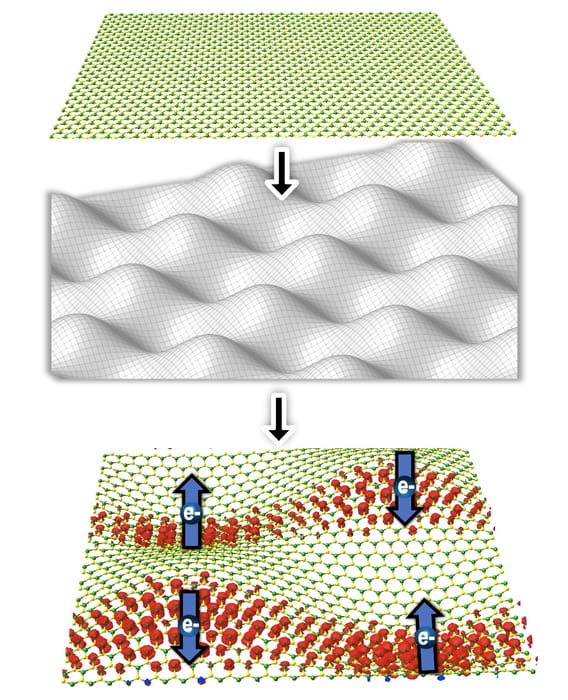
In the new work, a team led by Boris Yakobson showed that simply stamping or growing a 2D material on hBN onto a bumpy surface naturally strains the material’s lattice, creating pseudo-electric and magnetic fields that can then be used to control its magnetic and electric properties without a need for twisting. The researchers found that the strain creates “flat” band states that cause the normally insulating hBN to become a semiconductor. These states are 1D in nature, which is radically different from those obtained in twisted materials and could be exploited to study the exciting physics of 1D quantum systems, they say.
The advantage of the technique, which the researchers describe in Nature Communications, is that the deformation can be precisely controlled by using standard processes such as electron beam lithography to create patterns on the surface. “Indeed, it would be much easier to create bumpy surfaces using this process than it currently is to twist 2D bilayers of graphene or other heterostructures like hBN to less than a single degree of accuracy,” says Sunny Gupta, a postdoctoral researcher at Rice and a co-author of the study.
The researchers developed a computational model of deformation that they compare to wrapping a sheet of paper around a ball. “It is impossible to do this without crumpling the paper,” Yakobson explains, “because of their different topography (curvature patterns). To make it adhere to the ball, the sheet of paper should, in principle, be significantly deformed (if tearing is not allowed). Similarly, a flat 2D material when grown or stamped on a substrate with different topography will be strained and its electronic properties modulated.”
Creating different strain patterns
Using this model, the team found that substrates with different topographies could be used to create different strain patterns, giving rise to new quantum states and functionalities that are inherently absent in a flat 2D system, Yakobson adds. “By combining topography and deformation (which is like a adding a new ‘dimension’ in a 2D material) as we show in our work, we can create new quantum phases, such as flat electronic bands and strongly correlated 1D electronic sates,” he tells Physics World.
Strain switches 2D phase-change transistor
Such states, which are coveted by physicists, typically show unique properties such as magnetism and superconductivity. Creating them artificially is a highly active research field, but it is hard to do so via twisting because twisted systems require two layers of material and careful control of the twist angle between them. In contrast, the new technique can be employed even in single-layer materials. “Our proposed way of combining topographical modulations and 2D materials will overcome several limitations of current Moiré systems and allow us to explore physics in 1D systems, which is largely inaccessible by twisting 2D materials,” Yakobson concludes.
Using topography to alter the property of 2D materials is a new research direction, and in Yakobson’s view its broad scope means it could eventually garner similar attention as 2D twisted bilayer systems. “In the next stages of our work, we would like to explore how topographical undulations affect properties of a variety of 2D materials with inherent functional properties such as magnetism and electronic topological behaviour,” he reveals. “Importantly, we would also like to experimentally realize the material physics system we have offered the ‘recipe’ for in this study.”


