Topological insulators have shot to fame in recent years following observations of exotic phenomena like the quantum spin Hall (QSH) effect in quantum wells made from mercury telluride (HgTe). However, research on these materials, which are electrical insulators in the bulk, but which can conduct electricity on their surface (via special surface electronic states), is being held back for lack of high quality samples. Researchers in Germany and France have now developed a new wet-etch technique to make micron-sized (Cd,Hg)Te/HgTe structures that does not damage the samples and leaves the crystalline structure of the material intact.
The (Cd,Hg)Te/HgTe could be used for fundamental research on the QSH effect, in which spin-polarized electrons at the edges of an insulator are able to conduct. The QSH effect is interesting because it could be useful for making spintronic devices, which exploit both the spin and charge of the electron. As well as finding applications in such devices, the material might also be used as robust topological quantum bits (qubits) for quantum computers.
New fabrication scheme does not damage microstructure of topological materials
“Dry-etching processing techniques (such as ion milling) typically used to make topological insulators damage the sides of the samples,” says Laurens Molenkamp of the University of Würzburg, who led this research effort. “This is problematic when the quantum states you want to study are located exactly at these edges.” Ion milling can also lead to doping in these materials making them conducting in the bulk. “This is less of a problem in HgTe-based samples, however, which are better than most other topological materials in this respect – if processed properly, bulk doping in HgTe is very low.”
Molenkamp together with colleagues at the Ecole Normale Supérieure, PSL Research University in Paris, have put forward a new fabrication scheme that does not damage the microstructure of topological materials. Their chemical wet-etch process, which makes use of a solution of KI/I2/HBr to oxidize telluride (Te2-), leaves the crystalline structure of the material intact, producing samples of (Cd,Hg)Te/HgTe with a high carrier mobilities of 400 x 103cm2/(V s). The researchers calculated the mobilities by measuring how thin flakes of the material conducted electricity and found that the conductance of the different samples was almost independent of their thicknesses. This result is consistent with the picture that bulk (Cd,Hg)Te/HgTe is only conducting at its surface.
Higher mobility and QSH quantization over longer distances than ever before
“Wet etching techniques leave much cleaner edges, but because all known wet etchants for II-VI semiconductors are diffusion-limited, it is very difficult to make small samples using these etchants,” explains Molenkamp.
“What we have done now is carefully optimize a wet-etching recipe that does allow us to make micron-sized samples – with nice well-preserved edges. This shows up in the higher mobility of these small samples and quantum spin Hall quantization over much longer distances (over 10 μm along the sample edges) than possible previously,” he tells Physics World.
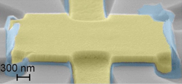
The researchers, reporting their work in Nano Letters 10.1021/acs.nanolett.8b01405, also used their samples to make high-quality Josephson junctions, which will allow for fundamental topological superconductivity studies in the future, they say.


