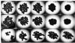
Nanocolloidal hydrogel scavenges heavy metals
Gels join forces with graphene quantum dots to decontaminate water
 Read article: Nanocolloidal hydrogel scavenges heavy metals
Gels join forces with graphene quantum dots to decontaminate water
Read article: Nanocolloidal hydrogel scavenges heavy metals
Scaffold-, label-, nozzle-free technology offers rapid fabrication of complex human tissue and organs, and could even be used in space
 Read article: Magnetic levitation promises to speed up tissue fabrication
Samples could be used to study the quantum spin Hall effect as well as to make spintronics devices and qubits
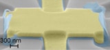 Read article: Wet etching makes high quality topological superconductor
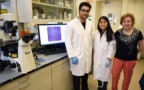
Researchers have found that the nanostructures reduce alpha-synuclein fibrils in mice
 Read article: Could graphene quantum dots help treat Parkinson’s disease?
Aqueous trapped ions could allow for nanofluidic computing say NIST researchers
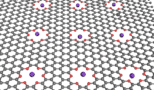 Read article: 2D sheets help make liquid logic
Computer modelling offers new insights into the printability cell-laden biomaterials
 Read article: 3D bioprinting simulations help optimize bioinks
The semiconductor could be a “revolutionary thermal management material”
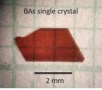 Read article: Boron arsenide crystals could cool computer chips
A new neonatal passive lung assist device shows promise
 Read article: Double-sided microfluidic blood oxygenator makes artificial placenta
The London brothers may have been right
 Read article: Static electric field suppresses superconductivity
Model describes how individual stiches in a knitted fabric behave when stretched
 Read article: New knit theory could help make smart self-folding materials