A team of researchers in Korea claims to have synthesized the most perfect large-area single-crystal graphene film ever by pinning down the temperature above which unwanted folds naturally develop in the carbon sheet. The new fold-free film will likely be used to make high-performance electronic and photonic devices.
Pure samples of graphene (a sheet of carbon just one atom thick) are usually grown using chemical vapour deposition (CVD). In this technique, a metal substrate is allowed to react under vacuum with volatile carbon-containing precursor chemicals, and a thin layer of pure carbon forms on its surface. While CVD is good for making high-quality graphene sheets with relatively large areas (a few centimetres on a side), the resulting samples generally contain some imperfections. These can include grain boundaries, regions with additional layers (adlayers), wrinkles and folds, all of which can degrade the material’s performance.
Compressive stress is the culprit
For scientists in search of ultrapure graphene, wrinkles and folds have proven especially tough to eliminate. These imperfections arise from the compressive stress created by the thermal contraction of the metal substrate on which the graphene is grown. As the materials cool down after the high-temperature CVD process is complete, this stress is partially released, and the resulting “de-adhesion” process produces wrinkles and folds in certain regions of the graphene.
Previously, researchers led by Rod Ruoff from the Center for Multidimensional Carbon Materials (CMCM) at the Institute for Basic Science within the Ulsan National Institute of Science and Technology (UNIST) in Korea discovered folds even in adlayer-free graphene grown on single crystalline copper metal foils. Their measurements showed that these folds are three-layered structures in the graphene sheet that vary in width from ten to hundreds of nanometres. They form parallel to each other at separations of about 50 to 100 microns, and sometimes run for centimetres in length.
While some researchers have reported obtaining graphene without folds – by, for example, using metal film substrates with a lower coefficient of thermal expansion – no group had achieved fold-free graphene films on metal foil substrates. The distinction between foil and film is important because metal foils have many advantages over conventional metal films: they are cheaper; easy to scale up to larger sizes and can be grown by stacking many of them in parallel over a single growth run.
Restricting the growth temperature
Ruoff and colleagues now say that they have produced large areas of single-crystal, fold-free monolayer graphene films on a metal foil substrate by restricting the temperature at which the material is grown to between 1000 K and 1030 K. To do this, they performed a series of experiments in which they used a mixture of ethylene with hydrogen in a stream of argon gas as the precursor to grow graphene on copper-nickel (Cu-Ni) foils developed in their laboratory. By repeating this process at different temperatures (including 1020 K), they determined the temperature at which folds form.
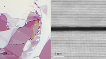
The researchers then used a technique called low-energy electron diffraction (LEED) to show that their fold-free graphene films form as single crystals over the entire growth substrate because they have a single orientation over a large area. They supplemented their LEED results with several other measurements, including transmission electron microscopy performed by UNIST graduate student Myeonggi Choe, a member of Zonghoon Lee’s group at UNIST, to confirm the presence of large area, single crystal, fold-free graphene.
Single crystal with essentially no imperfections
To test the electronic properties of the new material, the team prepared field-effect transistors (G-FETs) from it and found that the devices boasted very high electron and hole mobilities (around 7 × 103 cm2/V/s). Importantly, they observed that the G-FETs could be configured in any direction and at any location within the graphene sheet, with the mobilities of all the G-FETS remaining remarkably similar – a feat not achieved with other graphene films to date. “Such remarkable performance is possible because the fold-free graphene film is a single crystal with essentially no imperfections,” says team member and UNIST graduate student Yunqing Li, who was responsible for this part of the study.
The researchers also showed that they could grow their graphene on five foils (measuring 4 × 7 cm) at once, with each foil yielding two identical pieces of high-quality fold-free film on both sides of the foil. The graphene can then be removed, or delaminated, from the foils in about a minute using a technique called electrochemical bubbling transfer and the Cu-Ni foils can quickly be readied for a new growth/transfer cycle, says team member and UNIST graduate student Meihui Wang. Indeed, Wang found that the team’s 80:20 Cu-Ni(111) foils can be reused over and over once the graphene has been removed from them.
Ultra-flat graphene goes wrinkle free

Study co-author Da Luo and colleagues say their high-quality material could be used to make advanced devices with improved electronic properties. “The fold-free sheets can likely also be stacked more easily – either with themselves or sheets made from other two-dimensional materials, something that could further the range of potential applications,” they conclude.
The team, which reports its work in Nature, is now undertaking further studies with this graphene. “We expect to report on these experiments after more is learned,” Ruoff tells Physics World.