‘Plutoids’: the new name for Pluto-like dwarf planets

The International Astronomical Union (IAU) has decided that Pluto — and other dwarf planets in the Solar System that share similar characteristics — should now be sub-classified as “plutoids”.

The revised classification comes almost two years after Pluto was demoted from “planet” to “dwarf planet” in order to dispel inconsistencies in Solar System nomenclature that have arisen as more orbiting bodies have been discovered.

A dwarf planet is a body orbiting the Sun that has enough gravity to assume a near-spherical shape, but that is not the sole occupant of its orbit. To be a “plutoid”, according to the IAU, the dwarf planet must also be orbiting at a greater distance than Neptune. Aside from Pluto, the only other known dwarf planet fitting this specification is Eris, although more are expected to be found in the future.

The IAU, which has been responsible for the classifying planetary bodies and satellites since the early 1900s, had always planned to create sub-classes within the class of “dwarf planet”. The name “plutoid” was proposed by the IAU Committee on Small Body Nomenclature, and then accepted by the IAU Working Group for Planetary System Nomenclature and the board of IAU’s Division III, which concerns planetary systems. It was finally approved by IAU executives at a recent meeting in Oslo, Norway.

Still criticized

When Pluto was first reclassified, some astronomers criticized the definition for not being robust enough, in particular because the orbits of certain planets — including Earth — also overlapped with other bodies. On top of that, they complained that there were not enough astronomers consulted when the decision was made.

Catherine Cesarsky, president of the IAU, dismisses such past protests. “They form a very small part of the astronomy community,” she told physicsworld.com. She added that “practically nobody” is now trying to get Pluto reclassified as a planet.

However, Alan Stern, principal investigator for NASA’s New Horizons mission to Pluto, has already mocked the new plutoid definition. “Plutoids or haemorrhoids, whatever they call it. This is irrelevant,” he has been reported as saying.

Cesarsky admits that she has not yet heard the response from the astronomy committee for the rebranding. “I don’t think there will be a big [reaction],” she says. “A few people make a lot of noise.”

Astronomy in the dock

By Hamish Johnston

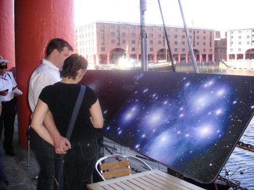
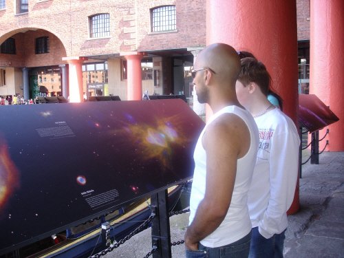
Earlier this week our Paris correspondent Belle Dumé was back in her hometown of Liverpool, where she took in an exhibition of astronomy images on display around the city’s famous Albert Dock.

Belle took a selection of photos and reported back to us.

albert%203.jpg

Called “From Earth to the Universe“, the exhibition runs until 29 June 2008. Belle says that it provides a taste of things to come during the International Year of Astronomy celebrations next year.

2009 has been proclaimed the International Year of Astronomy (IYA2009) by the International Astronomical Union (IAU) and UNESCO. Its mission is to bring astronomy into the wider public domain.

albert%202.jpg

Belle tells me that the new exhibition, sponsored by the Science Photo Library and the ASTRONET Symposium, is probably the first real IYA2009 event and consists of 48 stunning images taken by professional as well as amateur astronomers. These include photographs of our Milky Way, the Andromeda galaxy, the horse head nebula and the now famous image of the Cosmic Microwave Background revealed by the Wilkinson Microwave Anisotropy Probe (WMAP) satellite in 2003.

Belle’s hometown was chosen to host the exhibit because it is the European Capital of Culture this year. The exhibition also coincides with a major European astronomy meeting, the ASTRONET Symposium, which will take place from 16-19 June at the Liverpool John Moore’s University.

albert%201.jpg

Belle tells me that the display is a prototype for an exhibit that will tour the world next year. So it might be coming to a park, shopping centre, metro station or airport near you.

There will be special coverage of IYA2009 in upcoming issues of Physics World.

Going once…a first edition of Copernicus’s magnum opus

Copernicus%20book.jpg

By Jon Cartwright

Most of you will never have raised an arm at Christie’s auction house. But, if you’re partial to the odd extravagance, there’s a first edition of Nicolaus Copernicus’s De Revolutionibus Orbium Coelestium (“On the Revolutions of Celestial Spheres”) up for grabs. It’ll probably cost you around a million dollars.

Bidding for the 1543 volume starts on 17 June, and I expect it will end up in the vault of some blasé collector. No-one will ever read it, but then it is in Latin, and who understands that these days? Nil desperandum, though, that’s what I like to say.

Still, I know of least one physicist who would love to get his hands on it. Owen Gingerich, a historian of astronomy from Harvard University, has spent years tracing copies of Copernicus’s masterpiece, partly as an exercise for a book he wrote in 2004. A first edition would be the darling possession on his mantelpiece. “There aren’t that many copies in private hands these days,” he lamented on the phone to me a few moments ago.

Nowadays Gingerich finds solace in a second-edition. Although considerably less valuable, it does have annotations by Rheticus, the young mathematician who persuaded Copernicus to publish his radical ideas. Gingerich did get the opportunity a few years ago to buy a bona-fide first edition for $50,000, which would have been a good investment but which unfortunately would have required him to re-mortgage his house.

Will Gingerich put in a bid at Christie’s this time round? “I figure that even if I had it I’d have to rent a bank safety deposit box to keep it in,” he says. “So I’ll give it a pass.”

GLAST blasts off in search of gamma rays

The GLAST gamma-ray telescope was launched into space at 12.05 p.m. local time from Cape Canaveral in Florida today. The instrument is due to orbit some 560 km above the Earth’s surface where it will begin its survey of gamma rays from throughout the universe. Physicists involved in the project hope that GLAST (the Gamma-ray Large Area Space Telescope) will help them study some of the most violent events in the universe, provide a new window into the early universe and even shed light on the origins of dark matter.

The four-tonne observatory is packed with state-of-the-art particle detectors including GLAST’s primary instrument — the Large Area Telescope (LAT), which will cover the energy band between 20 MeV and at least 300 GeV. A second instrument, the GLAST Burst Monitor (GBM), will detect transient sources such gamma-ray bursts and solar flares down to energies of just 8 keV.

It took a lot of people in many countries to make this 16-year journey come to fruition Peter Michelson, Stanford University

GLAST must operate in space because gamma rays cannot penetrate even a few kilometres through Earth’s upper atmosphere. It is, though, possible to do some gamma-ray astronomy with ground-based telescopes by measuring the particles the gamma rays produce when they strike the matter in the atmosphere. However, such telescopes can only detect gamma-rays with energies of less than 100 GeV.

Gamma-ray bursts

One objective of the mission is to gain a better understanding of the origins of gamma-ray bursts. These poorly-understood events occur at a rate of about one per day, and briefly shine as the brightest objects in the universe. GLAST could allow to scientists to measure the total energy released in such bursts and the nature of their high-energy spectra — both of which have never been done.

GLAST will also target extreme events that occur in active galaxies when matter is accelerated to relativistic energies in a jet powered by a supermassive black hole. This results in the emission of gamma rays with a power equivalent to that of all the stars in an entire galaxy over all wavelengths. Until now, gamma-ray detectors have not been able to measure these highly variable emissions in any detail over long timescales, but GLAST will allow physicists to see into these jets, thus revealing their contents and dynamics.

GLAST will also support research in several areas in fundamental physics. One such opportunity is provided by the diffuse gamma-ray cosmic background — a poorly-understood haze of giga-electron-volt gamma rays that theorists currently attribute to cascades from distant tera-electron-volt gamma-ray sources, ultrahigh-energy cosmic rays, and even Hawking radiation emitted by primordial black holes.

Another area concerns one of the most fundamental questions in cosmology: the origin and distribution of dark matter. An important class of theories predicts the existence of weakly interacting massive particles, or WIMPs. In most models, WIMPs may annihilate in pairs, thus producing high-energy particles, including gamma rays. GLAST could be capable of detecting this radiation from annihilation events in the galactic halo, providing unique information about dark matter.

$690m price tag

The mission cost $690m and is a collaboration between NASA, the US Department of Energy and universities and research institutes in the US, Japan, Italy, France and Sweden.

“It took a lot of people in many countries to make this 16-year journey come to fruition,” says Peter Michelson, a physicist at Stanford University and principal investigator for the LAT.

Over the next two months the GLAST’s instruments will be tuned and calibrated. “First light”, when the telescope takes its first image of the sky, should happen in about four weeks and GLAST should start gathering data by mid-August.

Update 12 June 2008

After a 75 minute flight, GLAST settled into orbit and both of its solar arrays were deployed successfully.

Microscience 2008 offers a hands-on approach to microscopy

The event is organized by the UK-based Royal Microscopical Society (RMS), and will open with a plenary lecture from Sir David King, who was science and technology advisor to the UK government from 2000 to 2007 and is now director of the Smith School of Enterprise and the Environment at the University of Oxford. King, who is also professor of chemistry at the University of Cambridge will speak on “The 21st century challenges of sustainability and well being”.

Other plenary speakers include the Nobel laureate and nanotechnology pioneer Sir Harry Kroto, who will speak on “Mechanisms of self assembly at nanoscale dimensions”, on 25 June. Knut Urban — who is director of the Ernst Ruska-Centre (ER-C) for Microscopy and Spectroscopy with Electrons in Jülich, Germany — will deliver a lecture on aberration-corrected microscopy, also on 25 June.

The main programme of the conference is divided into three symposia that cover “Characterization and nanofabrication of advanced materials”; “Microscopy at the frontiers”; and “The cell in space and time”.

The advanced materials symposium includes sessions on in situ TEM and nanotechnology; advances in focussed ion beam microscopy; and nanopatterning and nanofabrication. Sessions on aberration-corrected electron microscopy and synchrotron-based microscopy will be included in the frontiers session. Not surprisingly, the cell in time and space will focus on biology and will include two sessions on “Imaging little to large: macromolecules to whole organisms”.

Free admission to exhibition

Microscience 2008 also includes a commercial exhibition that will feature close to 100 companies and admission to the exhibition alone is free. Participating firms include US-based Veeco Instruments, which will be introducing its HarmoniX atomic force microscope (AFM) at the event. JPK Instruments of Germany will be demonstrating its ForceRobot single-molecule force spectroscopy system, which is designed to make automated real-time studies of molecular interactions on nanometre length scales.

Among those firms showing off their latest optical instruments, Carl Zeiss of Germany will be exhibiting its new laser-scanning microscopes — the LSM 710 and LSM 710 NLO. Elsewhere in the exhibition, Canada’s Quorum Technologies will be introducing its Angstrom Grid Confocal System, which it touts as an alternative to laser-based confocal microscopes for examining fluorescent biological specimens. Other firms exhibiting at Microscience 2008 include the electron microscope makers FEI and JEOL UK and Hitachi.

Event organizers claim that a major attraction at the exhibition will be the RMS Learning Zone. This is a series of hands-on demonstrations covering four areas of microscopy: scanning electron microscopy; light microscopy; digital microscopy; and confocal microscopy. Participants will be able to meet experts in the respective fields and will receive a certificate of attendance.

The SEM portion of the Learning Zone will include a number of different instruments ranging from compact bench-top models to full-sized instruments. The microscopes are supplied by JEOL UK, FEI, Hitachi and Carl Zeiss and will be fully operational and ready to be used by exhibition visitors. This part of the Learning Zone will also feature two daily talks on how to prepare samples for analysis, followed by hands-on demonstrations. Participants are invited to bring their own samples for analysis.

The digital microscopy part of Learning Zone will include a number of workstations where participants can explore various methods including image capture; measuring morphometric and densitometric parameters; and the application of multi-dimensional imaging.

Optical microscopes supplied by Leica Microsystems, Meiji Techno, Olympus and Carl Zeiss will be available for use in the light microscopy area of the Learning Zone. Advice on both transmitted and refected light microscopy will be available from RMS experts.

The fourth Learning Zone will focus on confocal microscopy, and two instruments will be available for use — one supplied by Carl Zeiss and the other by Perkin Elmer. The microscopes will be used to demonstrate a range of techniques including multi-channel imaging, Z-stack formation and 3D/4D reconstruction.

Series of workshops

Microscience 2008 also includes a series of about 20 workshops organized by exhibiting companies. These include a session on multibeam imaging by JEOL UK and another on the geological applications of the SEM from Carl Zeiss. The Centre of Excellence in Metrology for Micro and Nano Technologies (CEMMNT) — a UK-based consortium comprising BAE Systems, Coventor, QinetiQ, the National Physical Laboratory and Taylor Hobson — will be running a workshop on how to link microscopy techniques to materials characterization methods. A workshop on creating 3D images over macroscopic scales — but at SEM resolutions — will be presented by Gatan UK.

The conference and exhibition both run over the full three days of the event, with the exhibition opening at 9:45 each morning.

Collaborations drive innovation at JEOL UK

When you sell a microscope that focuses electrons into a 0.1 nm diameter beam — which then must be held steady on a single column of atoms — you don’t just drop the instrument at your customer’s door and let them get on with it. Indeed, long before the system is packed for shipping, customer and supplier will have already collaborated on preparing an appropriate location where the instrument will perform at its best. Some of the customer’s personnel will have even been trained in how to use the instrument.

But according to Mike Hepburn, who is managing director of the UK subsidiary of the Japanese microscope maker JEOL, some of the firm’s customers actually help the company to develop microscopes at its factory in Japan.

Take Angus Kirkland, a materials scientist at the University of Oxford in the UK. JEOL is working with Kirkland’s research group to develop ultrahigh resolution transmission electron microscopes (TEMs). This has involved development staff from the firm’s manufacturing facility in Japan visiting Kirkland’s lab for several months at a time.

Hepburn told physicsworld.com that both parties gain from this type of interaction, with the Oxford group even publishing a number of research papers on the development of “super resolution” techniques for TEM. For its part, Hepburn says that JEOL can now offer technology developed in collaboration with Oxford on TEMs that it sells to other customers.

Making new science possible

According to Hepburn, a key achievement of the collaboration is that the TEM — which was originally specified to have a 0.12 nm resolution — is now operating at 0.07 nm. “That doesn’t seem like a huge difference numerically”, he says, “but in terms of the new science it makes possible, it really is a big difference”.

Other collaborations between the firm and UK universities focus more on developing new applications for JEOL instruments. This includes the company’s current collaboration with Pratibha Gai, who is JEOL Professor of Electron Microscopy at the University of York in the UK. Gai is one of the leading authorities on environmental TEM and co-director of the York JEOL Nanocentre, a £5.5m facility that opened in April 2007 and was partially funded by JEOL.

According to Hepburn, the centre is home to one of the world’s most powerful electron microscopes. This is a “double aberration-corrected microscope”, which has both imaging (TEM) and probe (scanning TEM) aberration-correctors fitted. It can obtain images at 0.1 nm resolution and resolve column of atoms at a resolution better than 0.2 nm.

The York researchers are using the instrument to develop new techniques for environmental TEM, in which a sample is placed in a small cell that does not need to be held under a high vacuum as with an ordinary electron microscope but can operate at ambient pressures. This technique allows researchers to see, for example, chemical reactions occurring in real time. “We help our customers through advanced training to understand the instrument so they can develop new applications,” explains Hepburn.

Elsewhere in the UK, JEOL maintains an ongoing relationship with Peter Goodhew, a materials engineer at the University of Liverpool and director of the superSTEM project at the nearby Daresbury Laboratory. SuperSTEM is developing two aberration-corrected TEMs — one of which is an existing TEM that has been retro-fitted with an aberration-correction system and the other which was delivered earlier this year by the US-based firm NION.

Corrected columns

While JEOL is not involved directly with the superSTEM project, Hepburn said that it is important for the company to be associated with one of the key groups working in this area “[Liverpool] is one of the leading groups for using corrected columns”, he explains. “We are very excited to be working with them”.

JEOL UK also collaborates with Tony Cullis, a semiconductor physicist at the University of Sheffield. The Sheffield group has recently ordered an ultra-high resolution TEM from JEOL, which is currently developing the instrument and expects to deliver it by mid-2009. To ensure that Cullis’s team will be able to use the new instrument when it arrives, JEOL is currently installing an interim instrument that will be used to train the staff.

“Our collaborations often begin with the development of leading-edge instrumentation and establish a close working relationship between the user and our development team”, says Hepburn. He believes that this delivers advantages to both parties. “We get feedback from the researchers back into the factory for future design and development and they benefit from getting advanced information about new developments,” he says. “In some cases we arrange for researchers to visit our factory in Japan to have discussions about design. It is a genuine win-win situation for both sides.”

Selling instruments

While collaborations with high-profile researchers help the company to develop new technologies, Hepburn emphasizes that JEOL is in the business of selling instruments to a wide range of users. He believes that there is much more to a successful sale than simply delivering the instrument. “It is one thing to encourage an institute to buy your instrument, but if it not sited correctly, or their staff not trained, then they are going to be disappointed”.

As a result, the company works very closely with the customer to ensure that its microscope is installed in the best possible location. “We get involved in the very beginning by having our engineers attend the customer’s site meetings”, explains Hepburn. JEOL engineers will even talk to architects and builders regarding alterations to existing buildings and the design of new facilities. This is important because environmental factors such as vibrations can have a detrimental effect on the operation of an electron microscope.

“We have been lucky enough at Oxford to have a new purpose-built building, but that is the exception rather than the rule”, he explains. “Normally we have to work within the confines of an existing building, which means that sometimes a hole has to be dug, then insulated from its surrounding area and filled with a solid concrete block” in order to minimize vibrations.

“Within JEOL UK we have several people who project manage the installation process from a technical point of view and our engineers have many years experience with creating the best location for an instrument,” says Hepburn. Although he admits that knowing what the correct environment should be is “a little bit of a black art”, Hepburn insists that the company will always get the right answer.

40th anniversary

JEOL UK has about 40 employees, with its parent company JEOL Ltd of Japan having 3250 people worldwide. JEOL Ltd was established in Japan in 1949, while JEOL UK was launched 40 years ago this year. According to Hepburn, the firm has installed more than 1000 electron microscopes in the UK — along with several hundred NMR instruments and mass spectrometers that the company also makes.

The vast majority of the company’s sales and service staff have scientific or engineering backgrounds, and many have been students or technicians in university labs that use JEOL instruments. This includes Hepburn, who worked in the Materials Department at the University of Surrey where he used a JEOL TEM.

Hepburn says that the firm is seeking to boost its ranks by hiring people at the postdoc level, who will help the firm expand its user-training and applications-development programmes. The company is also looking to sponsor the research of up-and-coming scientists who use their equipment. In doing so, the firm hopes to encourage the next generation of microscope users, as well as benefit from the drive and enthusiasm of less established researchers.

DAFNE enjoys a particle boost

Scientists at the Italian particle accelerator DAFNE are looking forward to an era of new physics having implemented an upgrade that is boosting the rate at which the machine can collide electrons and positrons. Their success paves the way for a new accelerator that is over 10 times as big with 10 times more energy.

The upgrade, which was completed five months ago, has already doubled the luminosity of DAFNE’s electron–positron collisions. Over the coming months the scientists think that it should be possible to make the luminosity three to six times higher.

“It’s increasing as we speak,” says Pantaleo Raimondi, project leader and researcher at the National Institute of Nuclear Physics, during a phone interview. “More luminosity means a higher collision rate, more particles and therefore more physics.”

Luminosity is increasing as we speak Pantaleo Raimondi, DAFNE

DAFNE is a compact, circular accelerator based at the Frascati National Laboratories, near Rome. It has two storage rings, each 100 m long, that accelerate electron and positron beams to energies of 0.5 GeV. At one point in the rings the electrons and positrons are extracted and then smashed into each other, before the remainders of the beams are re-entered into the ring.

The collisions produce phi-mesons, short-lived particles that contain a strange quark bound to a strange anti-quark. By studying the decays of these mesons — particularly into lighter kaons — scientists at DAFNE have been able to spend the best part of a decade studying aspects of particle physics such as quantum chromodynamics and CP violation.

‘As we hoped’

When it was built in 1997, DAFNE was deemed the world’s first particle “factory” because of its copious output of phi-mesons. The aim of the upgrade, which was implemented over the latter half of last year, was to see whether this factory could be made far more productive for minimal cost. If the upgrade was a success, it would prove the concept for a “super factory” called SuperB — a larger circular accelerator that will investigate the decays of heavier B-mesons. “Everything is performing exactly as we hoped, as we expected,” says Raimondi.

The upgrade has altered the geometry of the electron and positron beams to collide them at more of an angle. Although intuition would say that head-on collisions would give the highest luminosity, this arrangement leads to so much disruption that only a small remainder of the uncollided beams can be salvaged to re-enter into the rings.

An oblique collision reduces the disruption, but it comes with its own side-effect: it deters the beams from colliding at the point where the accelerator’s magnets force them to be thinnest. Raimondi and his team came up with the idea of giving the beams a “crabbed waist” — essentially tilting and rotating them — to make this thin point accessible again.

The upgrade has required around 60% of DAFNE’s rings to be modified at a cost of just €1.5m, which is modest considering the €150m value of DAFNE itself. The engineers are currently improving the accelerator’s detectors to exploit the large volumes of phi-mesons so that their decay processes can be measured more accurately.

‘Stepping stone’

With the upgrade already providing significant increases to DAFNE’s luminosity, the INFN and other institutions can concentrate on the design of SuperB, which will be constructed nearby. “It’s fantastic news,” says Tim Gershon at the University of Warwick, UK. “It’s a very important development in accelerator physics. It has immediate applications at DAFNE that could revitalize the programme. And it’s an important stepping stone for the SuperB factory.”

By putting all of these various things together we can get sets of measurements that complement those at the LHC Tim Gershon, University of Warwick

The measurements of B-meson decay processes will be important in testing particle physics beyond the current Standard Model. The behaviour of B-mesons is influenced by virtual particles that pop in and out of existence by borrowing energy from the vacuum, giving researchers a handle on particles that are too heavy to be produced directly (see this month’s Physics World feature: “A taste of LHC physics”).

There are already experiments looking into B-meson decay processes, including the Belle experiment at the KEK laboratory in Japan and the BaBar experiment — which was recently shutdown — at the Standford Linear Accelerator Centre in the US. There is also the LHCb experiment, which will start when the European laboratory CERN brings the Large Hadron Collider (LHC) online later this year.

SuperB, however, will be able to look for physics that would otherwise be out of reach. For example, it will be able to measure the decay of a B+-meson into a tau-lepton and a tau-neutrino — a process that the LHCb is not sensitive enough to measure.

In general, the B-meson factories give a different approach to direct particle searches, such as the LHC’s ATLAS and CMS detectors. “By putting all of these various things together we can get sets of measurements that complement those at the LHC,” says Gershon.

Force-microscopy firm finds success in 3D

When physicists Roger Proksch and Jason Cleveland founded Asylum Research in 1999, little did they know that nine years later one of their atomic force microscopes (AFMs) would be featured in one of the most successful US television programmes of all time — Crime Scene Investigation (CSI).

The company’s Molecular Force Probe-3D was used to produce a high-resolution image of a drug capsule found during a murder investigation in the episode “Rock and a hard place” of CSI: Miami. While the real-life applications of the firm’s systems are perhaps not as sexy as an appearance on CSI, Proksch told physicsworld.com that he continues to be surprised by the growing number of ways that researchers are using Asylum’s equipment.

Before founding the company, Proksch and Cleveland worked at US-based Veeco. However, the firm was becoming increasingly focused on making metrology equipment (including AFMs) for the semiconductor industry — something that didn’t appeal to the two physicists.

Dabbled in biophysics

“We were interested in making instruments for biophysics at the time,” recalls Proksch. Although the pair both did PhDs in the use of AFMs to study magnetic materials (Cleveland at the University of California at Santa Barbara and Proksch at the University of Minnesota) they had a growing interest in biophysics, having both “dabbled” in the field as postdocs. So they joined forces with lawyer Dick Clark to found Asylum Research, which has its headquarters in Santa Barbara, California. They now have about 60 employees, including many with PhDs in physics.

The firm’s first instrument was not an AFM, but rather a system that allowed biophysicists to measure the forces that hold large molecules together. This is done by attaching one end of the molecule to a substrate and the other to the tip of a tiny cantilever. The cantilever is then used to carefully pull the molecule apart, while the forces required to do so are determined by monitoring minute deflections of the cantilever.

This technique is called single-molecule force spectroscopy and can be used to study the structural properties of a wide range of large molecules such as DNA or polymers. Smaller molecules can also sometimes be studied by engineering them into larger molecules — using the larger molecules as “handles” to pull on the smaller molecules.

In 1999 the technique was only a few years old, recalls Proksch: “For us it was a nice niche, it allowed us to do something that was related to our experience but new enough that there was no competition”. The company ended up selling about 70 force spectrometers, the vast majority going to university biophysics research labs. Asylum had hoped that its instrument would become a diagnostic tool in the pharmaceutical industry. “But that just hasn’t happened and I’m not sure it will ever happen for this technology”, says Proksch.

Customer requests

By about 2002, sales to universities were beginning to slow down and Asylum saw its next opportunity in a request that it was getting from many of its customers — the ability to precisely scan the tip in the x–y direction, as well as up and down. Although the height of cantilever above the substrate could be positioned with nanometre accuracy, the instrument had relatively low resolution in the x–y plane. This meant that the user couldn’t know for certain exactly where on the molecule they where pushing or pulling.

“Our customers were asking us to make a system that could create an image of the molecule before you started poking at it — and that is basically an AFM”, says Proksch.

Fortunately, Asylum could use some of the same technology it had developed for the accurate positioning of the height of the cantilever to scan it in the x–y direction across the sample. This led to the development of the firm’s current “flagship” instrument, the MFP-3D. “One of the strengths of this instrument is that you can take these wonderful images of the sample and then you can go back and examine the other properties at specific locations”, says Proksch.

Proksch puts much of the firm’s success down to its use of linear variable differential transformer (LVDT) position sensors for use in its instruments. An LVDT comprises a primary coil with a current flowing through it to create a magnetic field. Some of the magnetic flux passes through two secondary coils, inducing currents in these coils. One contact of the position sensor is connected to the primary coil and the other contact to the two secondary coils. If the distance between the contacts changes, so does the relative positions of the coils and this change can be determined by measuring and comparing the induced currents in the secondary coils.

This is unlike its competitors, which use sensors based on capacitive plates to determine the position of the cantilever, if they use a sensor at all. The main difference between Asylum’s LVDTs — which use mutual inductance between magnetic coils — and low-noise capacitive sensors is that the latter require plates that are very large and in a perfect parallel planar configuration, which is very difficult to achieve, according to Proksch. “Magnetic coils are much more forgiving in terms of geometry”, he explains.

Low-noise amplifiers

Most LVDTs use a primary coil with a ferromagnetic core, which increases its magnetic field thereby boosting the sensitivity of the sensor. However, the sensitivity of this structure is limited by “Barkhausen noise” in the core, which results in sudden random changes in the magnetic field. To get around this problem, Asylum does not use a core in its patented LVDTs, but rather boosts the sensitivity of the secondary coils by using the latest in extremely low noise amplifier technology.

As a result, the sensors have noise level of about 0.1 nm noise in a 1 kHz bandwidth, which means that the instrument can make one position measurement per millisecond with an uncertainty of 0.1 nm.

While capacitive sensors claim to offer similar noise levels, Proksch says that they are much more difficult to integrate with an AFM. LVDTs, he says, can be used in a number of different geometries, giving Asylum considerable flexibility in designing their instruments — something that can be used to improve their overall performance. “We are the only AFM maker that I know of that takes this magnetic approach”, says Proksch, adding “I believe we are the only company that makes its own position sensors and this gives us the expertise to put our sensors just about anywhere”.

Growth in materials science

By creating instruments that scan in 3D, the firm has expanded its customer base beyond biophysics — which today is about 40% of its business — and has enjoyed significant growth in materials science.

The study of the piezoelectric properties of materials is one area where Asylum has seen significant growth. Piezoelectric materials generate an electric potential when squeezed or stretched — and such materials squeeze or stretch themselves when an electric potential is applied.

Although physicists have long known that many common materials are piezoelectric — including bone, wood, and many minerals — it had been very difficult to make detailed studies of the relationships between the microscopic structure of a material and its piezoelectric properties. This is particularly important to researchers trying to develop ferroelectric memories, in which data are stored in bits defined by the electric polarization of tiny domains in a ferroelectric material.

Today’s ferroelectric memories have a relatively low density and to improve this, researchers must be able to reduce the size of ferroelectric domains in the material.

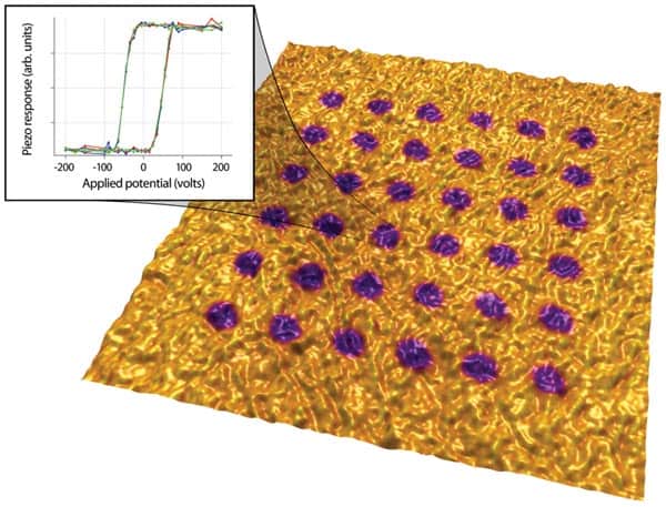
An AFM can be used to study the piezoelectric properties of a material by bringing the tip in contact with the surface, applying an electric potential between the tip and the material, and then measuring any movement in the material by watching for a deflection in the position of the tip. This technique is called piezo force microscopy or PFM.

According to Proksch, the MFP-3D can be used in piezoelectric scanning mode to image ferroelectric domains at resolutions down to several nanometres and garner additional structural information about ferroelectrics that could lead to denser ferroelectric memories.

Understanding ‘bioelectricity’

Beyond the development of ferroelectric memories, Proksch believes that the piezoelectric response of biological materials is a new and exciting area of growth for Asylum’s AFM. The piezoelectric properties of bone, for example, could be related to healing processes, whereby structural changes in damaged bone send out electrical signals telling surrounding cells to increase bone mass. As a result, such studies could lead to a better understanding of the role of “bioelectricity” in living organisms.

Proksch told physicsworld.com that the company is also currently working on reducing the time that it takes to obtain an image, which is typically about five minutes. This can be done by increasing the oscillation frequency of the tip, which in practical terms means making the cantilever smaller. While this is straightforward in principle, in practical terms it means that the rest of the hardware and software on the instrument also operate much faster — which is a significant challenge that the firm hopes to meet.


Microscopical advances redefine science

Mark Rainforth is professor of engineering materials at the University of Sheffield in the UK and has been involved with the UK-based Royal Microscopical Society (RMS) since he was a PhD student. His research involves using electron microscopy to study the interfaces and surfaces in metals, ceramics and coatings.

As president of the RMS since 2006, Rainforth oversees an organization that promotes every aspect of microscopy and allows all microscopists — users and instrumental developers alike — to interact. The society has over 1000 members including not just physicists, but also material scientists, life scientists, dentists and even archaeologists.

What have been the most exciting recent breakthroughs in electron microscopy?

There are so many that it is difficult to include them all. I remember going to a lecture a few years ago at which the speaker predicted that there was nothing exciting left to happen in microscopy and that all the changes would be incremental. In reality, over the past five years, the microscopy community has gone through a renaissance.

Perhaps the biggest advancement for me has been the ability to correct for the spherical aberrations that result from having round lenses. The resolution of a microscope has always been limited by such aberrations. People have known for a long time that the problems could be corrected by measuring the spherical aberrations and by using special lenses known as optipoles to put in equal and opposite aberrations. However, this requires many lenses and lots of image processing so has only really been possible with advances in computing power.

Before this it was only possible to produce an image that is a “projection” of atoms, rather than the actual individual columns of atoms in a material. Such a projection is made by recombining a number of diffracted electron beams to produce an interference image, which only under very carefully defined conditions gives us direct information regarding the atomic structure. Now, with aberration-free transmission electron microscopes, we can get true atomic images and get an idea of the physics of individual bonds between atoms.

In 1959 Richard Feynman famously said that, “It would be very easy to make an analysis of any complicated substance; all one would have to do would be to look at it and see where the atoms are…I put this out as a challenge: Is there no way to make the electron microscope more powerful?” Nearly 50 years later that challenge has been answered.

What other developments have been interesting?

The structures of many materials depend on their how atoms bond, something that must be studied at the angstrom (0.1 nm) length scale. But to understand how bonding affects what we can see with the naked eye, we must be able to make such measurements across much larger regions of a sample.

Electron back-scatter diffraction (EBSD) addresses this challenge by using a scanning electron microscope (SEM) to determine the crystal structure and crystal orientation of the atoms in a sample at the nanometre scale. The really exciting thing is that you can scan a wide area with SEM so you can cover a square centimetre of a material’s surface at nanometre-scale resolution.

This process is very computer-intensive and has only recently become possible with advances in computer power and digital cameras. Some of these latest techniques will be presented later this month in London at the Microscience 2008 conference.

Are these developments driving new science and technology?

Yes, but this is difficult to summarize because there are so many interesting cases. Indeed, it is almost like this renaissance has allowed us to revisit all known science.

Nanoscience and nanotechnology are widely recognized as having huge potential benefits. However, the technology cannot develop in a logical manner without the ability to probe atomic structure directly. This does not just mean the physical location of the atom, but also its atomic number and charge as well as the type of bonding with, and proximity to, surrounding atoms. Developments in microscopy are beginning to make this possible.

Microscopy also lets us manipulate objects on the nanoscale. For example, microscopes can be used to look at how a carbon nanotube can be moved into a specific position on a sample. In electronic components, we can now look at the interfaces between thin films and their substrates and understand the chemical distribution within the film. This understanding helps to further miniaturize the components leading to smaller mobile phones, for example.

Breakthroughs in microscopy have also boosted our ability to understand the effects of intentional or unavoidable trace elements in a material, which can dramatically alter its properties. Until the advent of the latest transmission electron microscopy (TEM) techniques, determining the locations of trace elements within the structure of a material was extremely difficult. Now, such microscopy techniques will, for example, bring new understanding in the degradation mechanisms in solid oxide fuel cells. Similarly, the development new high-strength, lightweight steels will also rely on the latest high-resolution techniques.

How is this renaissance in microscopy affecting your field of research?

My research focuses on the understanding of surfaces and interfaces. Microscopy underpins and explains all our work in materials science, be they metals, ceramics, coatings or biomaterials.

I use a range of techniques and sometimes need to combine more than one technique. For example, I use focused ion-beam microscopy to section surfaces for subsequent high-resolution TEM investigation. One situation where this is used is in examining the dynamic changes that occur in hip joint prosthetics while in the body.

What are today’s challenges in microscopy and how are they being addressed?

The current challenges cross many length scales, from achieving true atomic resolution, through to being able to find key features at the microscopic level, embedded randomly in a large object.

For atomic resolution, the first generation of aberration correctors have provided wonderful advances in resolution and therefore understanding. The next generation of (fifth-order) aberration correctors and chromatic aberration correctors, along with new electron gun designs, will in a few years’ time take the spatial resolution of electrons to a new level. Single atom electron spectroscopy should become almost routine. Such technology will also be built into SEMs, bringing major advances in the understanding of surfaces.

At the other end of the length scale, automatic stages coupled with advanced image analysis and related techniques, such as high throughput electron backscatter electron diffraction will bring major advances in the ability to resolve fine scale structure in a statistically meaningful way. Such techniques will benefit engineering firms that make large items with properties that are determined by fine-scale structure.

The rate of change is quite remarkable in every aspect. I am amazed by the number of new techniques coming out and I fully expect to continue to be amazed in the future. What better time to be a microscopist?

Scanning electron microscopy rises to the challenges of the 21st century

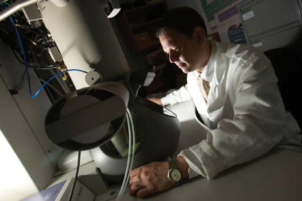
Since the first commercial instrument debuted in 1964, the scanning electron microscope (SEM) has become an established tool for characterizing materials in the physical and life sciences. SEMs are commonplace in the semiconductor industry, where they are used to create and characterize extremely small features, and the instruments are a key driver in the emerging business of nanotechnology.

The SEM is often seen as being less exciting than its counterpart, the transmission electron microscope (TEM), which can resolve individual atoms. Instead, SEM has a reputation as a workhorse instrument that is reliable, easy to use and ideal for characterizing bulk materials.

However, there has been a quiet revolution in the world of the SEM, and slowly but surely, its capabilities are expanding. The instrument can now be used to study the surface of just about any bulk material at nanometre resolution and regardless of whether it is clean or dirty, wet or dry, hot or cold, conducting or insulating. Under the most favourable conditions, sub-nanometre resolution has been achieved — especially for thin specimens imaged in transmission mode.

An SEM consists of a source of electrons that are focused by lenses into a tight beam that strikes the surface of a sample. The resultant signals from the sample — including backscattered electrons, secondary electrons and X-rays — are picked up by detectors.

Specimen as active component

Radical improvements in SEM capabilities have been brought about by new technologies such as field emission electron sources, magnetic immersion lenses, more efficient and sensitive detectors and specially adapted specimen chambers and stages. In addition, there is a growing awareness in the SEM community that performance can be boosted by treating the specimen as an integral, active component of the system.

So where does all this extra power get us? Well, it opens up a world of possibilities for tuning the experiment to match the specimen; to tease out the required information or to reveal the unexpected; and to use an SEM to fabricate structures at increasingly small scales.

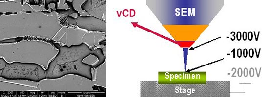
One strategy to improve the performance of an SEM is to apply a negative-bias voltage to the specimen, which slows down the incident (primary-beam) electrons on arrival at the specimen surface. These lower energy electrons don’t penetrate as deeply into the sample as a higher-energy primary beam would, and therefore are a more sensitive probe of the surface. The advantage of using a higher primary energy is that the beam can be made much more tightly focused, resulting in better spatial resolution.

Figure 1 shows this concept schematically, along with an image where the landing energy is a mere 50 eV, compared to the primary-beam energy of 2 keV. The reduced penetration of primary electrons into the material gives a much greater surface-sensitivity and, with the right detector, enables high-quality, low-voltage backscattered electron imaging (figure 2). This technique is unique in that it can provide high-resolution compositional and topographical information at the same time.

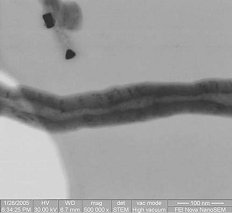
Another way of boosting the capability of an SEM is to position a detector beneath a thin specimen in order to collect electrons that are transmitted through the sample — similar to what is done in a scanning TEM (STEM). This “STEM-in-SEM” technique takes advantage of the comparatively low primary beam energies of the SEM (typically less than 30 keV), which means that more of the primary electrons scatter more often as they pass through the specimen.

This increased scattering makes it easier to study materials containing lighter atoms such as carbon, which are not very efficient at scattering electrons. This technique is particularly useful for studying polymers, carbon nanotubes (figure 3) and other organic matter.

Another exciting innovation is the environmental SEM (ESEM), which can also be used in STEM mode. “Environmental” refers to the instrument’s ability to image a sample in its “native state” rather than first being desiccated, coated in gold and held under high vacuum. The ESEM and microscopes using similar technologies are well suited to the study of electrically insulating bulk materials such as oxides, ceramics, glasses and polymer. Such materials would normally be electrically charged by the primary beam, making analysis very difficult.

The technique works by introducing an “imaging gas” such as water vapour to the sample chamber. When the primary beam strikes the sample, it produces ‘secondary electrons’, which ionize the gas, creating more secondary electrons as well as positive ions. The additional electrons serve to amplify the secondary electron signal, while the positive ions are attracted to the sample where they compensate for negative charge deposited by primary electrons.

Wetting and drying cycles

If water vapour is used as the imaging gas, the sample chamber becomes a suitable environment for stabilizing liquid-containing specimens and performing in situ experiments — for example, a sample can be studied as it is put through cycles of wetting and drying. Specimens can also be heated, cooled, stretched, compressed and otherwise manipulated, in association with a range of gases appropriate to the experiment. Recent advances in detector design mean that experiments can be carried out at chamber pressures up to around 4 kPa. While this is not quite atmospheric pressure (101 kPa), the pressure in a normal SEM is typically about one million times lower than this.

The SEM is also playing an increasingly valuable role in the fabrication of nanometre-scale devices for electronics and other applications. For example, interactions of the electron beam with specific gases can be used to achieve the controlled deposition of materials such as metals or different forms of carbon onto a substrate. This technique can be used to build 3D nanostructures or to create connections between nanocomponents.

Another method for making extremely small features using an SEM is electron-beam lithography. This process uses the electron beam to “draw” circuit patterns onto a substrate that is coated with a polymeric photoresist. The surface is then subjected to chemical etching, which removes the polymer that has not been exposed to the electron beam. Deposition and etching techniques can also be combined in a gas-mediated environment, as in the ESEM, leading to new and important techniques for creating nanostructures.

SEM analysis can be enhanced by the integration of a focused ion beam (FIB), which is scanned across the sample much like the electron beam. The FIB can be used to remove material from the surface of the sample (a process called milling), which allows the electron beam to probe deeper into the material. This sequence is repeated a number of times to obtain a number of 2D “slices” through a material, which can later be volume-rendered to create a 3D image. Slices can range in thickness from the nanometres to micrometres, depending on the size distribution of features present in the material. These abilities can be coupled with traditional analytical techniques such as electron backscatter diffraction (EBSD) and X-ray microanalysis (EDS) to build up 3D images of the structural and chemical properties of the sample.

This brief survey has shown how the modern SEM can take us from the advanced characterization of hard and soft materials, even liquids, to 3D visualization, dynamic experiments and the fabrication of nanostructures. Much of this is possible thanks to the extremely high level of control offered by the SEM — an ability that has evolved through decades of technology development coupled with increased computing power and dedicated software. In a cutting-edge world, the not-so-humble SEM is rising magnificently to the challenges of the 21st century.

Copyright © 2026 by IOP Publishing Ltd and individual contributors