Researchers in the UK and Africa have developed a quick and cost-effective way to determine the age of malaria mosquitoes using mid-infrared spectroscopy. This is important for assessing the effectiveness of control interventions as only older mosquitoes can transmit the parasite. The scientists say that their approach could also help with other mosquito- and insect-borne diseases.
According to the World Health Organization, there were around 241 million cases of malaria globally in 2020, killing more than 620,000 people. The vast majority of these were in Africa, which was home to 95% of malaria cases and 96% of malaria deaths.
Malaria is transmitted by female Anopheles mosquitoes. Strangely, the average lifespan of these mosquitoes is shorter than the time it takes for the Plasmodium parasites that cause malaria to develop. This means that only a small proportion of mosquitoes live long enough to pass on the disease. Because of this, malaria control interventions such as insecticidal nets tend to target adult mosquito survival. An accurate and reliable method of determining the age of the insects would help assess the impact of such vector controls. The current way to do this involves dissecting mosquitoes’ ovaries. This is expensive, slow and hard to do at scale.
In recent years, there has been some success using infrared spectroscopy to determine the age of mosquitoes. This technique provides information regarding the chemical composition of the insect’s cuticle (its protective exoskeleton), which varies with species and age, based on the light signature returned when it is illuminated with infrared light. But while this approach is accurate for laboratory-reared populations that are genetically similar, spectroscopy has struggled with ageing genetically diverse wild mosquito populations.
Now Francesco Baldini, a medical entomologist at the University of Glasgow, and his colleagues have combined mid-infrared spectroscopy with deep learning to develop a rapid, cost-effective way to identify the species and age of three species of malaria carrying mosquito. They report their results in Nature Communications.
“With this infrared technology, we have developed a tool which could be adopted within current mosquito control plans, has the potential to be scaled up for use across different areas, and would greatly help in testing new products and solutions against diseases transmitted by mosquitoes,” Baldini says.
The researchers used data from more than 40,000 female mosquitoes of different ages from three malaria-transmitting species. The insects came from diverse genetic backgrounds and were reared both in different laboratories and semi-wild conditions in East and West Africa to capture genetic and environmental variations. The artificial intelligence (AI) model was initially trained using mid-infrared spectroscopy data from the genetically varying lab-reared mosquitoes. The team then retrained it using an additional sample of mosquitoes from the semi-wild populations. The resulting model was able to predict the age and species of mosquitoes reared in semi-wild conditions from their mid-infrared signatures with more than 95% accuracy.
To further test the effectiveness of this “transfer-learning” approach, the researchers collected wild mosquitoes in Burkina Faso and Tanzania. They then dissected and age-assessed a sample of these and used them to retrain the AI model that was previously trained on the lab-reared mosquito populations. When tested on more of the wild mosquitoes, this deep-learning mid-infrared spectroscopy system returned similar results to traditional dissection techniques.
Baldini says that the technique requires mosquitoes to be collected, killed and then scanned in a laboratory. Mosquitoes are already routinely collected in many areas to check species and malaria infection rates. “The [spectroscopy] procedure takes approximately 10 seconds per mosquito instead of several hours and is essentially free after the upfront cost of the hardware,” he explains.
“We envision this approach could also be applied to other vectors and vector-borne diseases, from filariasis and chikungunya, to sleeping sickness and Zika; and could be used to evaluate the attempts to limit the expansion of invasive mosquito species across Europe and the United States,” says Baldini.
In the future, it may even be possible to scan flying mosquitoes. Baldini notes that this will probably be easier using near-infrared spectroscopy, rather than mid-infrared. “We are working on the development of this type of device,” he adds.
From TNT to nitro-glycerine, nitrogen-rich compounds are known for packing an explosive punch. When these materials explode, bonds between atoms in the compounds are broken, which gives a chance for two nitrogen atoms to form very strong triple bonds with each other. This releases an enormous amount of chemical energy due to the high strength of the triple bond, which is almost six times stronger than its single-bond counterpart. In fact, the strength of nitrogen-nitrogen triple bonds is one of the reasons that the stable nitrogen gas dominates Earth’s atmosphere.
This chemical property of nitrogen is encouraging scientists to develop new nitrogen-rich compounds for use as high energy-density materials that can be used as explosives or propellants. Polymeric nitrogen exists in the form of chains and tubes of linked nitrogen atoms with a high number of single or double bonds that can break and form triple bonds, releasing a large amount of energy and no dangerous by-products.
Several types of these polymers have been made at high temperatures and pressures, but they have been notoriously difficult to stabilize at ambient conditions. However, the electrochemical pressure inside the confined walls of carbon nanotubes may be the key to realizing these structures under more practical conditions. In a paper, published in Chinese Physics Letters, a team of scientists led by Jian Sun at Nanjing University provide a theoretical map to the process and the resulting compounds.
Carbon nanotube nano reactors
When graphene sheets of a single layer of bonded carbon atoms are rolled up, they can form cylindrical molecules with a diameter on the order of nanometres, called carbon nanotubes. Like test tubes, high-strength and high-stability nanotubes can be used as containers for chemical reactions, as they are larger than simple molecules. But nanotubes are not just passive vessels, their small dimensions provide confinement effects that can help stabilize a reaction and even control it. Previously, scientists studied pre-made polymeric nitrogen molecules in nanotubes, yet most have not been fabricated directly in the tubes.
In their recent work, Sun and colleagues use a new computational approach to search and characterize potential polymeric nitrogen structures, like in the conceptual figure above. Modelling the potential inside simplified carbon nanotubes of different diameters, the software looks for possible polymerized structures using a machine learning approach called Magus. Then, the properties and stability of the structures were investigated using molecular dynamics simulations.
Their technique predicted that stable chains and tubes of nitrogen atoms can form in two previously known structures as well as three completely new ones. Both the pressure acting on the nitrogen chains and the confining potentials inside the carbon nanotubes of different sizes highly affect the type of nitrogen structure formed, and consequently its properties.
Polymer predictions
Not only did the researchers predict the existence and stability of different polymeric nitrogen structures, but they also describe their expected properties. Theoretical studies of their vibrational properties suggest the nitrogen structures are likely to be mechanically stable, with the stability being strongly dependent on the size of the nanotubes.
Simulations using models more closely resembling actual carbon nanotubes show that the carbon tubes might sometimes deform to having an elliptical cross-section, further stabilizing the nitrogen chains. Simulations of some of the polymeric nitrogen structures at room temperature suggest that they can be stabilized in bamboo-like nanotube structures. The electronic properties of the structures inside the nanotubes are predicted to range from semiconductors to more metal-like behaviour.
Importantly, the energy density of the polymeric nitrogen is expected to be almost twice that of TNT, suggesting their potency as propellants or explosives.
From theory to experiment
While the research provides an understanding of how confined structures could be used to stabilize nanomaterials, creating these structures in the lab will be a tough task. Using short nanotubes with sodium azides as precursors under laser heating and a mixture of argon and nitrogen might do the trick. Still, the realization of these structures remains a challenge to be faced by experimental chemists.
In this webinar, experts explore the possibilities of signal processing in response to the future challenges and opportunities of advanced measurement systems.
The speakers will cover a broad spectrum of topics ranging from basic to industrial research, organized in concise thematic sections that reflect the trends and impact of current and future developments per research field.
Left to right: Dimitris Iakovidis, Andrew Yacoot, Manus Henry, Silvano Donati and Jianghui Geng
Dimitris K Iakovidis is editor of the Roadmap on signal processing for next-generation measurement systems. He is professor at the University of Thessaly, Greece, and the director of its Biomedical Imaging Laboratory. His research focuses particularly on digital signal processing and medical decision support systems.
Andrew Yacoot is editor-in-chief of Measurement Science and Technology. He leads the dimensional nanometrology work at NPL and chairs the BIPMs Consultative Committee for Length’s Working Group on Dimensional Nanometrology.
Manus Henry is director of the Advanced Instrumentation Group at the Department of Engineering Science, University of Oxford, UK, and professor of flow management, Coventry University, UK. His interests include self-validating sensors and systems, particularly in flow measurement and enabled through signal processing.
Silvano Donati is an emeritus professor at the University of Pavia, Italy, with a wealth of experience in the application of laser diodes to optical techniques, particularly in the area of interferometry and noise limits. He is the inventor of self-mixing interferometry.
Jianghui Geng is a professor and director of the Satellite Navigation and Positioning Technology Research Center of Wuhan University, China. He is particularly interested in the challenges presented by multi-constellation and multi-frequency GNSS signal processing.
About this journal
Measurement Science and Technology was the world’s first scientific instrumentation and measurement journal. It covers all aspects of the theory, practice and application of measurement, instrumentation and sensing across science and engineering.
Editor-in-chief: Andrew Yacoot, National Physical Laboratory, Teddington, UK.
A simple colour change could indicate the presence of potentially hazardous hydrogen gas thanks to a new sensor developed by researchers in Germany. The micron-scale device, which uses so-called “supraparticles” that turn from purple to pink in the presence of hydrogen, could help prevent explosions by making it easier to detect and localize leaks at fuel stations, generators and pipelines.
Hydrogen produced using renewable energy is an environmentally-friendly fuel and could play an important role in the transition to more sustainable energy sources. It is, however, extremely flammable and potentially explosive in the presence of air, and its colourless, odourless nature makes it hard to detect. Optical hydrogen sensors tend to employ complex structures such as nanoantennas, light sources, optical fibres and electronic control devices to convert an optical signal into a readable response, while “gasochromic” (that is, colour-changing) hydrogen sensors are often fabricated as thin films of specific substrates, resulting in a fragile multi-layer structure.
Distinct two-colour change
A consortium of scientists at the FAU Erlangen-Nürnberg, coordinated by Jakob Reichstein in Karl Mandel’s research group, has now made an alternative hydrogen sensor using supraparticles with three components: silica nanoparticles, gold-palladium (Au-Pd) nanoparticles and an indicator dye called resazurin. The team combined these three ingredients in an aqueous dispersion that they atomized to generate small droplets. They then introduced the droplets into a hot chamber in a process known as spray-drying. When the solvent evaporates, Reichstein explains that the nanoparticles and dye molecules are forced together, forming a structure known as a mesoporous supraparticulate framework that is accessible to gases such as hydrogen.
As the particles in the structure absorb water from the atmosphere, they form a three-phase system that allows the resazurin molecules to propagate freely. In effect, Reichstein says that the water acts as a transport medium, carrying the resazurin dye molecules towards the catalytic active Au-Pd nanoparticles. In the presence of hydrogen, the resazurin is reduced (that is, it picks up a hydrogen atom), forming a related chemical, resorufin. If hydrogen continues to be present – as would be the case for an ongoing leak – an additional reduction reaction occurs, transforming the resorufin into hydroresorufin.
“The hydrogen-induced reduction of resazurin is accompanied by a distinct two-step colour change of the supraparticles: the first irreversibly from purple to pink and then reversibly to a colourless state,” Reichstein explains. “These changes can be seen with the naked eye.”
Simple structure
Reichstein says that the team’s hydrogen-indicating supraparticles have several possible applications. With diameters between 1-10 µm, the particles are small enough to be incorporated as additives or pigments in various materials, including coatings on pipelines and safety clothing. This makes it easy to exploit them for rapid detection of hydrogen and for precisely localizing leakages at almost any point of interest.
The researchers, who report their work in Advanced Functional Materials, plan to optimize their supraparticles until they can “realize their full potential, implement them in real-life applications and therefore make a contribution to a safer hydrogen economy”. “Currently, we are investigating and improving the sensitivity of the supraparticles as well as their long-term stability,” Reichstein concludes. “We are also testing the gasochromic functionality of the supraparticles in coatings.”
Communication and management skills are really important. I also lead group meetings, mentor students, manage projects, exchange ideas with peers and develop research projects. Travel and meeting people in-person are an exciting part of the job too. There’s not been much of that since the pandemic started, but hopefully we’ll come back to this soon.
What do you like best and least about your job?
I love working in large, international, cross-border teams, developing new technologies, understanding problems and pushing boundaries to shape the future. Educating students and training the next generation of quantum scientists in the lab is also a great part of the job. I find it fascinating to see students evolving and growing as scientists, and to learn with and from them. As for the bad parts, administrative work is not my strongest suit, and probably on my list of pet hates, although I understand that housekeeping is vital if I’m to do the best possible research. What’s also been hard is the string of back-to-back online meetings. They leave little time for creativity, but hopefully things will get less stressful as time goes on.
What do you know today, that you wish you knew when you were starting out in your career?
Obviously with any career you don’t necessarily know where it’ll take you. So most of the time during my own career I didn’t know what opportunities were waiting around the corner – it would have been useful to know what was coming next! I have also realized that academic research is all about new approaches, methods or experiments – and that it’s okay to try and fail. That’s what humans are all about: we learn from our failures. It’s important in my area of applied physics to be free to do experiments that might go wrong because only then do we learn the art of trying and trying until we get things right. That’s what eventually brings you success.
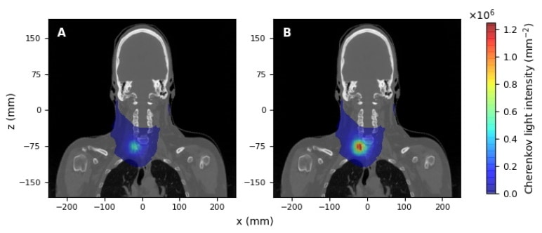
Developing a dosimetry technique: Spectrally-integrated Cherenkov light intensity at the patient surface for a molecular radiation treatment of papillary thyroid carcinoma, with radioisotope uptake distributed in the tumour. (Courtesy: CC BY 4.0/Biomed. Opt. Express 10.1364/BOE.448139)
Molecular radiation therapy (MRT) is a treatment in which radioisotopes given orally or intravenously are used to deliver radiation to diseased tissue. As with all radiotherapy techniques, successful treatment relies on accurate control of the dose to the target. But in contrast to external-beam irradiation, with MRT it is not possible to accurately plan the delivered dose, due to the lack of control over the uptake, retention and distribution of the radioisotope within tissue.
As such, there’s a real need for patient-specific dosimetry to assess the dose delivered to the treated tissue. Currently, however, MRT dosimetry techniques are limited. Addressing this shortfall, research led by the University of Surrey investigates whether measurements of Cherenkov light at the patient surface could be used for a new MRT dosimetry technique.
Cherenkov light is produced in tissue when charged particles travel at a speed greater than the phase velocity of light in tissue. In MRT, charged particles are created as the administered radioisotope decays. All of these charged particles deliver therapeutic dose, while only those with high enough phase velocity also produce Cherenkov light.
The relationship between the dose delivered to the tissue and the emitted Cherenkov light intensity is linear – a necessity for dosimetry based on Cherenkov light. Other requirements include a small inter-patient variability in this linear relationship and ensuring that the measured optical signal probes the treatment volume.
In a study reported in Biomedical Optics Express, the researchers investigated the effect of inter-patient variability in tissue characteristics and radioisotope uptake on the linear relationship between the dose absorbed by the treatment volume and Cherenkov light intensity at the surface of the patient.
“Our study showed how the spatial and spectral characteristics of Cherenkov light can be exploited to optimize the performance of a Cherenkov-based dosimetry technique,” explains first author Jigar Dubal from the University of Surrey.
Numerical experiments
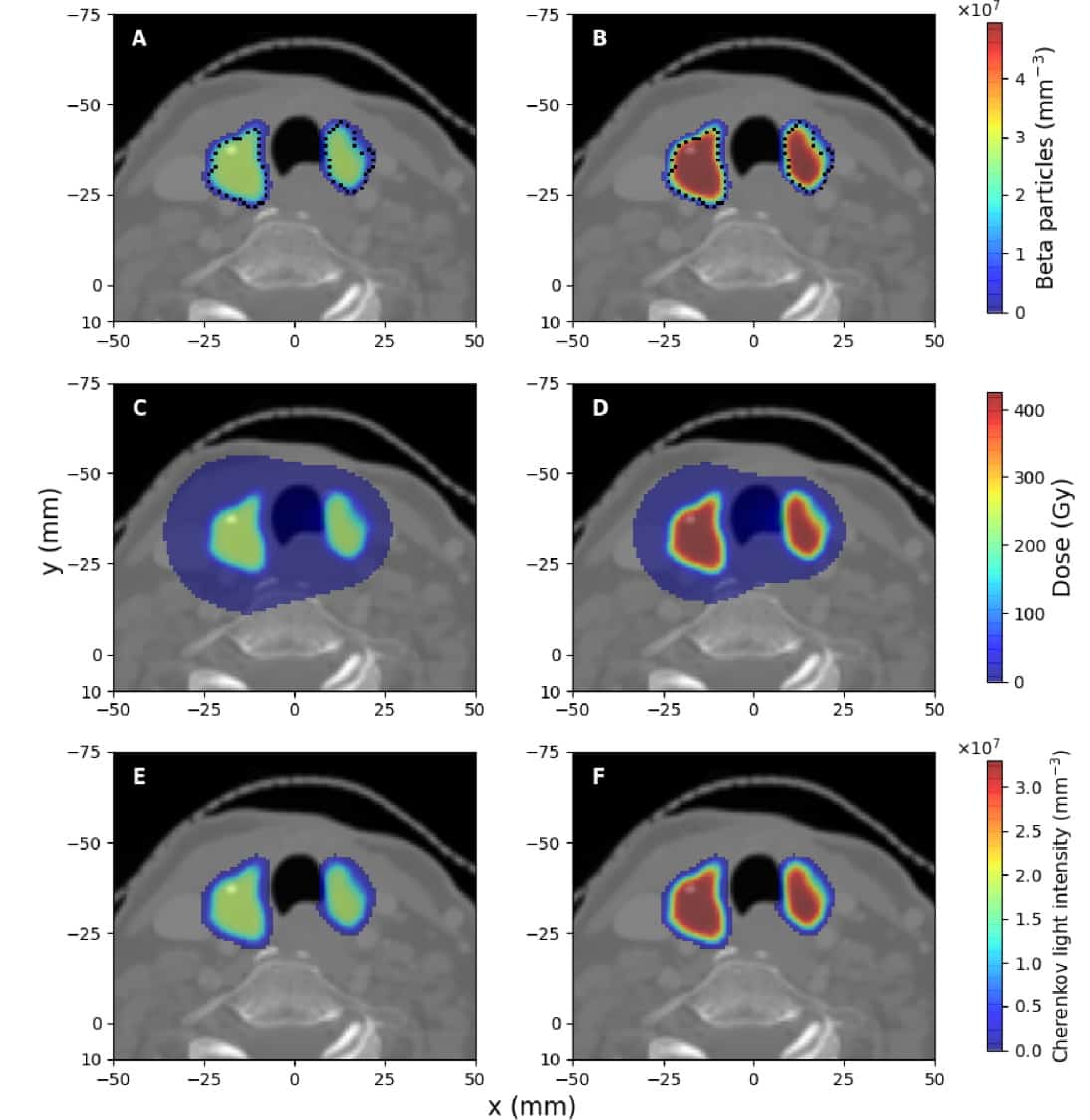
Dubal and colleagues simulated MRT using iodine-131 (131I), as employed clinically, to treat hyperthyroidism and papillary thyroid carcinoma (PTC). This radioisotope undergoes beta decay, producing electrons that deposit dose and generate Cherenkov light. They used clinical CT images to create the 3D patient geometry, with tissue types defined by the densities obtained from the CT scanner calibration curve. To model the light emission and propagation within the patient, they assigned optical parameters to each tissue type, and considered the inter-patient variability in these characteristics.
MRT of hyperthyroidism: Beta particles produced from 131I decay (A, B); absorbed dose (C, D); and Cherenkov light intensity (E, F), for 131I activities of 400 MBq (left column) and 700 MBq (right column). Courtesy: CC BY 4.0/Biomed. Opt. Express 10.1364/BOE.448139)
For hyperthyroidism, the simulations considered 131I spread throughout the thyroid gland. For PTC, the radioisotope was either distributed solely in the tumour or with some accumulation also in surrounding thyroid tissue, thus modelling the patient variability in radioisotope distribution. The team simulated 131I decay within the treatment volume to determine the spatial distribution of the beta particles, the deposited dose and the spectral and spatial characteristics of the Cherenkov light.
The simulations showed that the emitted Cherenkov light was localized in the treatment volume, with the light distribution mostly overlapping with deposited dose. While the light intensity varies linearly with the absorbed dose, this relationship is patient-specific, due to differences in patients’ tissue optical properties and, in the PTC case, radioisotope uptake.
The team next assessed the Cherenkov light emerging at the patient surface, which could be measured for dosimetry applications. In this study, while Cherenkov light is mostly emitted at lower wavelengths, simulations showed that surface light is predominantly in the near-infrared (where tissue absorption is minimal). In this spectral range, the Cherenkov light reaching the surface mostly originates in the treatment volume, and its spatial distribution exhibits areas of high intensity, dependent upon the position and symmetry of the treatment volume
The researchers also examined the relationship between the mean dose deposited in the target and the total Cherenkov light intensity, for measurements over the entire surface area and in a 25 x 25 mm hot spot. They demonstrated that the relationship between dose and light intensity was more robust to inter-patient variability (in tissue optical parameters and radioisotope uptake) when light was measured at the hot spot rather than over the whole surface, and more robust for PTC treatments than for hyperthyroidism treatments.
These findings could pave the way for patient-specific MRT dosimetry based on Cherenkov light measurements. To optimize the accuracy in estimating the mean dose deposited in the treated volume, the researchers recommend surface light measurements in the near-infrared spectral range and at the intensity hot spot on the surface
While inter-patient variability affects the dosimetry accuracy, the researchers note that the uncertainty in estimating the dose using Cherenkov light can be less than for current MRT dosimetry methods.
The team is continuing numerical experiments with the aim of devising a 3D dosimetry technique. “Using Cherenkov light could provide a more accurate and cost-effective alternative to existing dosimetry techniques for molecular radiation therapy,” says senior author Lucia Florescu. “We are currently considering utilizing multiple surface light measurements to reconstruct the 3D Cherenkov light distribution within the tissue, to gain insight about the 3D dose distribution and achieve comprehensive patient-specific dosimetry.
I’ve been passionate about electromagnetism since I was an undergraduate, and I also had an interest in nanotechnology. That was how I got started in nanophotonics, and specifically in plasmonics, which is an approach that enables us to confine and manipulate light on the nanoscale by exploiting interactions between electromagnetic waves and loosely bound electrons in metals. During my PhD, I learned that plasmonic structures, which are typically made of gold or silver, can be used to confine electromagnetic energy to very small volumes. That really rang a bell in my mind. Conventional optical tweezers trap objects at the focus of a laser beam, but the diffraction limit makes it challenging to focus light down to spot sizes less than about half the wavelength of light. That, in turn, limits the size of particles one can trap, and I could see that plasmonics might offer a way around this.
I quickly Googled “plasmonic tweezers” to see if anybody had done any work in the area. When I learned that they had, I began to think about what new contribution I could make. I realized that because the electromagnetic energy only extends a few tens of nanometres away from the surface of the plasmonic nanostructures, there is a challenge associated with the speed with which you can trap and manipulate particles using plasmonic tweezers. Typically, one has to rely on diffusion for particles to transport themselves randomly until they get close to “hotspots” in the electric field where they can be trapped. That’s a very slow process. It can take anywhere from several minutes to an hour before trapping occurs, depending on the concentration of the particles in the system.
In 2016 I published a paper (Nat. Nanotechnol.11 53) that addressed that problem for the first time, making it possible to trap nanoscale objects with plasmonic tweezers in less than five seconds. In that paper, we showed that plasmonic tweezers not only have the ability to tightly grip nanoscale objects, they can also act as a really long “arm” to transport particles from tens or even hundreds of microns away.
What do these plasmonic nano-structures look like?
There are different geometries that can be considered, but one commonly used one is a nanopillar – basically a tiny cylinder that sits on a substrate. That cylinder forms an antenna, so when you shine light on a surface fashioned in this manner, you can easily sustain a dipole mode where you have two hotspots at the two extremities of the nanopillar. Other designs look like a bowtie or a double nanohole aperture, and they are both very efficient at squeezing light to extremely tight volumes.
What applications become possible once you’re able to manipulate nanoparticles more easily?
There are two broad areas. The first is in the life sciences, and it relates to nanosized particles called extracellular vesicles. We used to think that these particles were just a means for cells to expel waste, but in the last couple of years, scientists have discovered that they contain functional molecules like proteins, DNA, micro RNA and messenger RNA. These functional molecules can be used to encode information and communicate with neighbouring or distant cells, so they are very important for therapeutics and as a way to monitor the progression of diseases like cancer via what’s termed a liquid biopsy.
The challenge is that they are very, very small, and they are also highly heterogeneous both in their size distribution (anywhere from 30 nm to about 1 µm) and in their biogenesis. They all have different functions, too, and crucially, if you want to use them for liquid biopsy (an application my group is actively investigating), you need to be able to detect protein markers and RNA molecules contained in individual vesicles. This is a key area where optical tweezers and nanotweezers can deliver new functionality, because conventional approaches such as high-speed differential ultracentrifugation only work for bulk samples. They don’t allow you to analyse vesicles and markers at an individual level.
We are very interested in developing a platform that enables us to manipulate single photons for use in quantum photonics
The other interesting application area is in quantum photonics. The key to this emerging field is the creation of single photons and entangled photons using a non-classical light source, but it’s a challenge to do this in a way that’s compatible with established silicon chip technology and not too complex. Another drawback is that the photon emission rate of nanoscale quantum emitters is too low for most practical applications. That means we need to couple them to structures with a high photonic density of states, so that their emission performance can be enhanced. Hence, being able to manipulate these nanoscale emitters, some of which are below 30 nm in size, presents another opportunity for optical nanotweezers.
Since 2020 you’ve developed specialist nanotweezers for both application areas; what are these devices and how do they work?
The first is called an opto-thermo-electrohydrodynamic tweezer, or OTET. It’s a very cool device and we published a paper about it in 2020 (Nat. Nanotechnol.15 908). The idea is that it’s incredibly difficult not only to trap sub-10 nm particles, but also to manipulate them. Regular optical tweezers cannot handle such small objects, and even plasmonic tweezers can only trap them right at a hotspot, where the temperature is high. That presents a challenge for delicate biological molecules like proteins or DNA. To keep those biological molecules intact, we needed a way to trap them away from high laser intensity, high-heat regions.
The way we do that with the OTET is to take a metal film and drill nanoscale holes in its surface. We then illuminate this structure with a laser such that some of the energy in the resulting plasmonic wave gets converted to heat. That produces a localized heating in an adjoining fluid medium, which in turn results in a temperature gradient in the fluid and a gradient in the fluid’s temperature-dependent properties such as electrical conductivity and permittivity. If we then apply an AC bias, we can induce electro-hydrodynamic flow in nanoparticles suspended in the fluid via the electrothermal effect. This electrohydrodynamic flow is basically a microfluidic vortex, and when you resolve it into its radial and axial components, you discover that the radial component is pointing inward.
The other effect involved in the OTET is called AC electro-osmotic flow. This phenomenon occurs because when we have this nanostructured metal film, and we apply an AC bias perpendicular to it, then in the region far away from the nanostructure, the electric field will be normal to the surface – that’s what Gauss’ law of electrostatics tells us. However, once you get close to the gold nanohole array, the field distorts so that there is a tangential component as well as a normal component. That tangential component can then act on the diffuse charges in the electrical double layer induced at the interface between the nanohole array and the fluid. When those charges move, they induce a fluid motion that carries the nanoparticle with them.
In OTETs, this AC electro-osmotic flow is radially outward, so we have a radially inward electrothermoplasmonic flow combined with a radially outward AC electro-osmotic flow. Together, these competing flows create a stagnation zone where the flow velocity falls to zero, and thus where the nanoparticle can be trapped. Once this trapping is established, we can then dynamically manipulate the particle simply by translating the laser beam. Crucially, the trapping zone is always several tens of microns away from the laser focus, which ensures that the particles never experience high laser intensity or photo-induced heating. The particles basically “feel” the ambient temperature, but you can still translate them from one position to another by moving the laser beam. It’s like action at a distance, something we might think of as science fiction, but we can make it happen in microfluidic chips.
What about the other device? I understand it’s designed to manipulate nanodiamonds with nitrogen-vacancy (NV) centres for quantum photonics applications.
This is our low-frequency electrothermoplasmonic tweezer, or LFET, which we described in a paper published in June 2021 (Nano Lett.21 12 4921). Nanodiamonds with NV centres have been found to be very stable quantum emitters for quantum photonic applications because they do not experience photobleaching (that is, exposure to light does not chemically alter them in ways that would change their emission properties). Single NV centres also make good single-photon sources. But to have the emission properties needed for these applications, the nanodiamonds need to be coupled to photonic structures.
Nanodiamond trap Rendering of the low-frequency electro-thermoplasmonic tweezer, or LFET. (Courtesy: Justus Ndukaife)
The LFET does this by leveraging an effect that is typically considered to be detrimental in plasmonics, which is that plasmonic structures dissipate heat. We use an AC electric field to induce an interaction between the nanoparticles and the plasmonic surface, which in this case is an array of gold nanopillars on a substrate. This interaction is very strong at low frequencies, and it enables us to trap single nanodiamonds. Then, when we illuminate a region of the gold nanopillars with light and apply an AC bias, we’re able to induce electro-thermoplasmonic flow to transport these nanodiamonds from several tens of microns away and position them close to the laser spot. Once they get close enough, they do experience some repulsive thermal force, but we’re able to mitigate that by using a low-frequency AC field.
The LFET enables us to move nanodiamonds from one region to another within seconds. In comparison, other approaches common to this area of quantum photonics, namely, the use of atomic force microscope (AFM) tips to pick up nanodiamonds and move them into position, are very tedious, taking up to or even more than an hour.
Optical nanotweezersallow us to analyse protein markers and RNA molecules contained in individual vesicles, which could help in the diagnosis of cancer
What’s the biggest obstacle you’ve had to overcome in developing these nanotweezers?
We’re an experimental group, even though we do a lot of computer modelling to understand the devices that we are designing or developing, and one of the key challenges we experience is in fabricating our nano-structures. Sometimes they don’t have the dimensions or morphology we need, and then we have to go back and re-do the fabrication. We often go through several iterations before we get all the parameters right. Once we’ve done that, though, the process becomes easier.
What’s next for you and your group?
With respect to quantum photonics, we are very interested in developing a platform that enables us to manipulate single photons. To that end, we are working to integrate nanoscale emitters with well-designed nanophotonic structures so that we can enhance single-photon emissions and route emitted photons on a chip.
For the biophotonics aspect, the key challenge we would like to address is to be able to analyse thousands of individual extra-cellular vesicles with very high throughput. This would be important both for our fundamental biological understanding of these particles and for the translational biomedical applications, which include liquid biopsies for non-invasive early disease diagnosis and monitoring patient response to treatment. An example might be certain kinds of cancer that are not accessible to conventional tissue biopsy techniques. It would be very beneficial if we could develop the capability to harness these vesicles, which are present in most bodily fluids (including blood plasma and saliva) to get information on the state of the cancer. That is something that will be very beneficial to society and will help to improve patient outcomes, and I believe there’s plenty of room for optical nanotweezers in this domain.
Researchers in the Netherlands and the US have shown for the first time that qubits – the building blocks of quantum computers – can be mass-produced using standard processes developed for manufacturing conventional integrated circuits. The breakthrough paves the way for developing powerful quantum machines that require thousands or even millions of identical qubits for full-scale operation.
Quantum computers promise a revolution. A large-scale quantum device could, for example, simulate chemical reactions involving thousands of molecules, thereby accelerating the development of medicines and new materials. To get there, however, quantum computers will eventually need millions of qubits, whereas today’s early-stage versions contain only a modest number – all of which must be manufactured in the laboratory.
Producing qubits on the same scale as the computer chips found in smartphones and other modern digital devices has proved elusive for several reasons. The processes that produce these conventional chips have undergone a decades-long trajectory of development and standardization. To benefit from these advances, large-scale qubit production must follow the same design and fabrication rules.
In principle, this should be possible for so-called spin qubits, which are made from the same silicon material as integrated circuits and work by controlling the spin of charge carriers (electrons and holes) in semiconductors. Spin qubits are, however, difficult to make and need to operate at temperatures below 4K to achieve long coherence times.
Going large
In the latest work, researchers at QuTech (a collaboration of TNO and Delft University of Technology) in the Netherlands, together with colleagues from Intel in the US, designed and manufactured silicon spin qubits using Intel’s state-of-the-art optical lithography 300mm wafer process line. Previous work to produce qubits on wafers had instead used electron beams to pattern the structures on the wafer, which is much slower. The optical lithography process, in contrast, uses equipment similar to that used for commercial integrated circuits, and made it possible to fit more than 10 000 qubit arrays on a single 300 mm wafer.
The researchers tested two properties of their processed wafer: device yield and sample uniformity. The former is measured by checking how many of the manufactured devices operate properly, with current flowing and contacts not leaking. The latter is measured by comparing the room-temperature threshold voltage of individual qubit gates. The results indicated a yield and sample uniformity of 98%, with consistent uniformity throughout the wafer and only a few devices at the edge not functioning. When the team repeated the tests at temperatures of 5K and lower, the results correlated well with those obtained at room temperature.
Advanced qubit fabrication
Lieven Vandersypen, a researcher at QuTech and a co-author of a Nature Electronics paper describing the work, says that this is the first time anyone has produced complete qubits using the same processes employed to mass-produce integrated circuits. He adds that the number of qubits produced is several orders higher than could be accomplished with laboratory equipment. More importantly, the yield is higher, as lab production has a failure rate “on a good day” of at least 50%. Vandersypen notes that the high yield is remarkable because the design rules of standard processes lack the flexibility that university cleanroom equipment provides, meaning that the process could reduce qubit quality if not properly designed.
Silvano de Franceschi, a researcher at CEA in Grenoble, France who was not involved in this work, says it is important that one of the leading manufacturers of microprocessors is now using its advanced fabrication facilities to make qubits. He is also impressed by the researchers’ efforts to correlate statistical device properties at low temperature with those measured in ambient conditions, noting that this is “important for optimization of the fabrication processes”. However, de Franceschi adds that electron beam patterning is more flexible for initial optimization and could have a similar yield if integrated in an industry-standard way. Furthermore, in his view the level of charge disorder in this first generation of qubits does not seem low enough to allow for large-scale qubit integration. “We are just at the beginning and there is certainly margin for improvement,” he says.
Vandersypen says that he and his colleagues now plan to increase qubit production still further. “We also want to improve the control over the qubits and test new concepts to increase the scalability,” he tells Physics World. In his view, the high reliability and volume of the new production process will enhance the rate of progress across the field.
Infrared night-vision systems that see in colour could be a reality thanks to researchers in the US, who have used machine learning to create colour images of photographs that are illuminated with just infrared light. The team hope their technique could be further developed to create imaging systems that operate where the use of visible light is impossible, such as retinal surgery.
Traditional night vision systems work by illuminating an area with near infrared radiation and detecting the reflections or by using ultrasensitive cameras to detect the small amount of light present even at night. Both, however, usually produce monochromatic images, so researchers are seeking ways to produce multi-colour images of objects without having to bathe them in visible light.
Computer scientist Pierre Baldi of University of California, Irvine (UCI), explains that this would be very useful in medical applications where use of visible light is problematic. “It is very toxic for the retina to receive light of high intensity for long periods of time,” he explains. “Surgery may last four hours – if you have high intensity, short wavelength light shining on the retina continuously for four hours, there is a strong chance the patient may become blind. At the same time, you would like the surgeon to see things as though they were irradiated with regular light.”
Multi-wavelength infrared illumination
Researchers had previously tried several approaches to colourizing infrared images, but these often required some knowledge of the visible image as an input or sacrificed image clarity for colour. In this latest research, Baldi and ophthalmologist Andrew Browne, also at UCI, set out to produce full-colour images from multi-wavelength infrared illumination. This would allow images visually indistinguishable from the originals while obviating the use of visible light.
To achieve this, they first printed a rainbow colour palette from a standard, three-colour office printer onto white paper and imaged the spectral reflectance under multiple wavelengths of visible and near-infrared light. After selecting six wavelengths – three in the visible and three in the infrared – they printed 200 images of human faces from a public database and illuminated all of them with each wavelength in turn, detecting the intensity of the reflected light.
The researchers then developed a computational deep-learning algorithm, in which a computer predicted the reflectance at the three visible wavelengths using the values of the reflectance from the three infrared wavelengths. This generated an image that was then fed to a “discriminator” that evaluated the predicted image against the reference image and tried to tell them apart. If it could do so, this information was fed back to the generator, which used this information to refine its predictions.
“At the beginning of learning, when the parameters are sort of random, it produced a completely random type of image,” says Baldi. “There’s a procedure for adjusting the parameters of both the discriminator and the generator using this information.”
Ever-more accurate
The system was thereby trained to produce ever-more accurate colour reconstructions of the visible image from infrared data in a feedback loop. “The basic algorithms are the same as are being used in all computer vision tasks – whether it’s self-driving cars, looking at images from satellites or whatever, the same techniques can be used in all these imaging problems,” Baldi says.
At the end of the experiment, the researchers asked humans to evaluate the visual quality of the images produced by their deep learning algorithm. They found that the images were consistently rated as clearer and more accurate than those produced by a simple linear regression algorithm, in which the intensity at each visual wavelength in turn was predicted from the intensity at one infrared wavelength.
Two important improvements are needed before the system can be used for medical applications. One is to boost the current data acquisition rate beyond the current three frames-per-second so that video imaging is possible. The other is to adapt the system so that it works with biologically relevant samples such as retinal tissues – which have different infrared reflectance spectra than the images used in this study. Beyond this, the researchers suggest that the work could have applications in security and military operations and animal observation. “You can imagine many follow-up steps,” says Baldi.
Whenever I talk to people about how I became a patent attorney, they seem surprised that I studied physics rather than law. However, my background is actually quite common in the profession, as a degree in a science subject is almost essential for the job. In my case, I moved into intellectual property nearly 10 years ago after doing a PhD in quantum computing at the University of Leeds in the UK, followed by a postdoc in the same subject at Louisiana State University in the US.
I explored what other opportunities were on offer and changed fields after realizing that a career in physics was not for me. At first glance, the switch from physics to patent law seems a big one, and it might seem like you’d have to first do a law conversion course. In fact, you don’t, and the transition is smooth as there is on-the-job training. Indeed, having a PhD or industry experience is often an advantage because inventors like to work with people from their own field.
If you think a career as a patent attorney is worth considering, there are several questions you are bound to have. Apart from the most obvious one – what exactly is a patent? – you’ll probably also want to know what do you do as a patent attorney? How do you enter the patent profession? And what sort of training is involved? I hope my answers to these questions give you a clearer idea of the profession and how to pursue it.
So what is a patent?
A patent is a form of intellectual property that protects an invention. In return for disclosing the details of the invention to the public through publication of a patent, the proprietor gains a monopoly right for a particular country. The scope of this monopoly right is defined by what are called the “claims” of the patent. The patent also includes a detailed description and diagrams of the invention.
What does work as a patent attorney involve?
I spend a typical day reading and writing about inventions, which makes for a fun job as you are constantly learning about the latest technology. Specifically, patent attorneys write patents – a process known as “drafting” – and work to achieve the granting of them by a patent office through a process known as “prosecution”. During drafting, a patent attorney will discuss the invention with the inventor, and write claims and a description of it. Having previously done research into quantum computing, I particularly enjoy working with inventors in that field, as I get to see things from both sides of the fence.
During prosecution, a patent attorney will edit the claims based on the description and provide written arguments about why the invention is new and clever. The prosecution process can also involve attending hearings at a patent office, where the attorney has to argue for the invention in person. I find it genuinely interesting to read technical documents in various fields and getting to understand them at a level where you can make arguments about them.
In addition to drafting and prosecution, patent attorneys sometimes also work with patent solicitors and barristers to ensure a patent has not been invalidated or infringed. They might also be involved in “freedom to operate” work, which involves checking if any existing patents would be infringed if a product were to get commercialized. Such tasks are particularly common if, like me, you work in a general law firm, rather than a patent-specific business. In-house patent attorneys at hi-tech companies may also be involved in licensing and managing their firm’s patent portfolio.
How do you get into the patent profession?
The vast majority of patent attorneys obtain a trainee role without having any patent-related qualifications, so it is worth applying for positions even if you do not have any qualifications in the area. However, if you want to train first, it is possible to do a Master of Laws (LLM) postgraduate degree in intellectual property law before you start.
Many patent attorney firms do have the equivalent of a graduate recruitment scheme, but they are usually smaller than similar programmes in other sectors and there are often only one or two trainees taken on per year. Some companies follow the typical graduate recruitment cycle, but it is not unusual for positions to start at any time of the year. Nevertheless, with interviews often being held in December or January, my advice is to get your application in before then if possible. And given that many firms do not have a fixed training cycle, positions may remain open longer or start dates may be more flexible than typical graduate schemes.
If you are interested in joining the profession, it makes sense to research a list of patent attorney firms on, for example, the IP Careers website. You can then apply either for particular openings or make a speculative application (unless a firm explicitly says it does not want people applying in that way). Many applications only require a CV and covering letter, but some ask for additional written work, such as a description of an everyday object, as part of the initial application.
If your application is successful, you will often be invited to an interview, although a few firms use assessment days. The interview will typically involve the standard job-related questions, but the employer may also ask you to give a presentation on some aspect of technology, such as your current research. In many cases, the interview will also involve another exercise that is more representative of the day-to-day work, such as describing an everyday object or figuring out how an invention works.
These question-and-answer exercises are designed to test how you think on your feet, so firms like to keep their interview questions secret and change them regularly. That said, as the questions are designed to test how you think, don’t panic if you don’t know the answer instantly. Just be prepared to work through them and see what you can do.
What training do you need to become a patent attorney?
Once you have a role as a trainee, most of the training occurs on the job. That’s because the exams you need to sit to qualify are designed to test your ability as a patent attorney. Most firms will also fund a set of external training courses and provide tutorials specifically geared towards the exams.
If you live and work in the UK, you will typically aim to become a UK patent attorney (which means you are a registered representative at the UK Intellectual Property Office) and a European patent attorney (which makes you a representative before the European Patent Office). Separate exams are required for each qualification.
To become a European patent attorney, you will sit an initial multiple-choice “pre-exam”, which you can take only after you’ve trained for at least two years. If you pass, you can sit the main exam, which consists of four “open-book” papers on different aspects of the job: patent law, drafting, amendment and opposition. Most trainees sit all four papers in one year, but this is not necessary to qualify. Traditionally, the exams were taken in person, but they moved online during the pandemic, which may be continued on a permanent basis.
To become a UK patent attorney, you’ll need to sit two sets of exams. The first, known as “foundation exams”, can be skipped if you’ve been on an accredited course (or obtained an accredited LLM in intellectual property). This is the route I took and many patent firms pay for their trainees to attend such courses. Some are part-time while others are almost full-time, meaning you essentially get three months off to study. Your firm should discuss this with you either before or after you have taken up a position.
The second set of UK exams, known as “finals”, consists of four papers, one each in patent law, drafting, amendment, and infringement and validity. You may be able to skip the drafting and amendment exams if you have passed the corresponding European papers, though whether you can do this will depend on your firm. Some don’t require you to sit drafting and amendment exams at all, while some firms say the drafting and amendment exams have to be sat at least once and some require you to resit until you pass. It is unusual to pass all exams first time so resits are not uncommon.
Once you have finally passed all the exams, you are a qualified patent attorney. However, on-the-job training never really stops – patent attorneys are always learning as that is the nature of the work. For me, I have really enjoyed my switch from academia to patent law, and I even get to work on patents related to quantum computing – the field I worked in. If you are considering making the switch and have any questions about life as a patent attorney, feel free to contact me and I will do my best to answer.