Optical tweezers have been used to manipulate nanoparticles within superfluid helium at a chilly 1.4 K. The experiment is described as the “first successful application of optical tweezers at ultralow temperatures,” by Yosuke Minowa – who achieved the feat along with colleagues at Osaka University in Japan. The researchers believe that their work could lead to a better understanding of the interface between the classical and quantum worlds.
When liquid helium is cooled to about 2 K, it transforms into a quantum state of matter that has zero viscosity and can therefore flow forever without any loss of kinetic energy. This superfluid helium has several curious properties, such as the ability to climb up the walls of a container and escape captivity. Furthermore, excitations such as vortices in the superfluid are quantized.
While superfluid helium has been studied extensively since its discovery 85 years ago, some of the physics behind superfluidity remains a mystery. Improving our knowledge of the phenomenon goes well beyond the bounds of the Earth because superfluidity is believed by some to exist inside neutron stars.
Focussed beam
One poorly understood area is how superfluids interact with objects such as nanoparticles, whose behaviour straddles the border between quantum and classical physics. In this experiment at Osaka, researchers introduced gold or zinc oxide nanoparticles (about 10–80 nm in size) to superfluid helium. This was done by firing a laser at a gold or zinc oxide surface that is immersed in the superfluid, knocking nanoparticles off the surface and into the superfluid.
Another laser beam was strongly focussed to a small region within the superfluid to create optical tweezers, which could hold the nanoparticles in place for up to 30 minutes.
Optical tweezers are an established technique that make use of the fact that the electric field gradient in a laser beam is greatest at the focal point and this attracts and holds nanoparticles. However, the team say that this is the first time that optical tweezers have been used at such low temperatures.
As well as offering a way to study interactions between classical and quantum physics, Minowa and colleagues believe that nanoparticles held in optical tweezers could provide a way of studying quantized vortices in superfluids. For example, the nanoparticles could be used to visualize or even control these quantum states.
I imagine astronomers are feeling pretty pleased with themselves. That’s because the James Webb Space Telescope (JWST) – the long-awaited successor to Hubble – is nearing the L2 Lagrange point, roughly 1.5 million kilometres from Earth, with all seemingly going to plan.
The JWST’s spectacular 6.5 metre primary mirror, which had been folded up on the telescope’s journey from Earth, has been unfurled, aligned and cooled, protected by a massive, tennis-court-sized sunshield. The first infrared images – yielding secrets of everything from exoplanets to the first galaxies – could be in by June.
More than 20 years in the making, the JWST has suffered its fair share of budgetary, operational and technical headaches – and further hitches cannot be ruled out. But one thing NASA has also had to contend with is a dispute over the mission’s name.
That’s because the mission is named after James Webb, a former NASA administrator who died in 1992. Webb has been accused of being involved in anti-LGBT+ activities before taking up the reins at NASA. He is also said to have been in charge when a budget analyst at the agency was sacked in 1963 on suspicion of being gay. More than 1200 people signed a letter last year demanding the JWST be renamed.
NASA declined to do so – prompting the resignation of a member of its astrophysics advisory committee. But similar demands are already being made elsewhere in physics. One such demand has come from Michael Pepper, a semiconductor physicist at University College London. In a letter to the Times in November, he said he thinks it’s time to rename the “Stark effect”, which describes the splitting of an atom’s spectral lines in an electric field.
The term honours the German Nobel-prize-winning physicist Johannes Stark (1874–1957), an anti-semite who was an early supporter of Adolf Hitler. He backed the notion of “German physics”, in contrast to the supposedly “Jewish” physics being developed by, among others, Albert Einstein. Stark received a four-year suspended sentence from a denazification court after the Second World War.
In light of this history, Pepper feels the Stark effect should be rebranded. “It could be called electric quantization or something like that,” Pepper said on a recent episode of the Physics World Weekly podcast. That doesn’t mean, he argued, we should strip Stark of his Nobel prize. “One can’t the change the past – and one shouldn’t even try – but we can change the future.”
In related news, a petition to rename the Schrödinger Lecture Theatre at Trinity College Dublin is now doing the rounds. The facility is named after the Austrian quantum physicist Erwin Schrödinger, who was based at Trinity from 1938 to 1955. During his time in Ireland, he is said by the Irish Times to have “indulged his Lolita complex”, grooming and sexually abusing two young girls.
“We can acknowledge the great mark Schrödinger has left on science and this petition does not wish to diminish the impact his lectures or ideas had in physics,” the petition states. “However, it seems in bad taste that a modern college such as Trinity could honour this man with an entire building.”
Some physicists might blanch at the prospect of combing through phenomena, statues, labs, buildings or departments for examples of other less-than-honourable honorees. Who next, they might wonder, will be “cancelled” from physics for incidents or episodes that might have happened decades or centuries ago? But on the other hand, if things are named after awful people, surely it’s better to make amends for these past wrongdoings now, rather than continuing to compound them?
A new nanomechanical resonator inspired by the structure of a spider’s web could be used in quantum sensors to sense ultra-small forces such as gravity. The resonator, which was designed using machine learning, works at room temperature – a first for a device of this kind.
Nanomechanical resonators are tiny vibrating beams that oscillate at very high resonant frequencies – often in the megahertz or gigahertz range. They are employed in a range of applications, including telecommunications, and can also be used to detect and determine the mass of tiny objects such as single DNA molecules or viruses. They work on the principle that whenever a small particle is absorbed onto the beam, the frequency at which the beam vibrates changes in a way that can be monitored and used to calculate the particle’s mass.
The ultra-sensitivity of these devices can work against them, however, as it makes them extremely sensitive to ambient thermal noise. As a result, such resonators need to be kept at temperatures near absolute zero (–273.15 °C) to counter these unwanted vibrations.
A team of researchers from TU Delft in the Netherlands has now made a resonator that works at room temperature thanks to its excellent isolation from external noise. The new device’s design was inspired by the structure of a spiderweb, which is one of nature’s best vibration detectors.
Spider silk threads are very tough and stiff, boasting strength-to-weight ratios on a par with steel. They are thus able to withstand large impacts while remaining sensitive enough to detect and trap small flying insects. Crucially, they are also most sensitive to vibrations emanating from inside the web, rather than from vibrational disturbances in the surrounding environment, such as wind.
This unique behaviour is the result of millions of years of evolution and thus represents a good starting point for machine-learning algorithms to design nanomechanical sensors, says Richard Norte, who co-led the new study together with Miguel Bessa.
Making use of Bayesian optimization
The researchers chose a popular mechanical-resonator material, silicon nitride (Si3N4), for their sensor. They used an algorithm known as Bayesian optimization to find a good spiderweb-type design quickly and efficiently, having first specified that the machine-learning programme should consider devices made from a slab of 20 nm-thick Si3N4 freely suspended over a length of several millimetres.
To their surprise, they found that the algorithm proposed a relatively straightforward web, one that consists of just six strings assembled in an apparently simple way. Better still, the team’s computer simulations showed that the device would work at room temperature due to its high mechanical quality factor, which is the ratio of energy stored in a resonator over the energy dissipated over one oscillation cycle. This quality factor, denoted Qm, exceeds one billion in this temperature range thanks to a novel “torsional soft-clamping” mechanism that isolates the device’s vibration modes from the ambient thermal environment and was discovered by the data-driven optimization algorithm.
“What is fascinating is that the machine-learning algorithm independently homes in on torsional vibration mechanisms, which are actually used by spiderwebs in nature when detecting prey, although the algorithm does not have any prior knowledge of how a spiderweb functions,” they explain.
The researchers then made a real-world sensor based on this optimized design, set it vibrating with piezoelectric stages and used an optical interferometer to measure the time it took for the vibrations to stop. These “ringdown” measurements provide information about the rate of decay of the resonator’s amplitude and so the rate at which it dissipates energy – values that are then used to calculate its Qm.
The researchers report that almost no energy is lost outside of their microchip-based “spiderweb”. “The vibrations move in a circle on the inside and don’t touch the outside,” Norte explains. “This is somewhat like giving someone a single push on a swing and having them swing on for nearly a century without stopping.”
Extending to other geometries
The new device could be used to search for dark matter or probe ultra-tiny forces such as gravity that are notoriously difficult to measure, the researchers say. While their initial design uses silicon nitride, they believe that their approach could be extended to other materials such as diamond, gallium arsenide, silicon carbide, indium gallium phosphide, fused silica glass, silicon, phosphorus carbide and even superconducting films. Using machine learning to design such devices is just a first step toward developing the next generation of nanomechanical resonators, the researchers add, and it might also be extended to geometries other than spiderweb-like designs.
Spurred on by their results, the team now plans to develop new machine-learning algorithms to design optical nanostructures rather than just mechanical ones. “These structures will be used to solve other physics problems such as creating lightsails that travel at a quarter of the speed of light,” Bessa and Norta tell Physics World. “They will require a careful design that allows them to be ultra-lightweight and highly reflective – characteristics that are difficult to achieve simultaneously.”
The energized state of living matter leads to the dynamic behaviour of billions of interacting nanometre-sized biomolecules, and the spatial–temporal patterns resulting from this collective behaviour give rise to cellular functionalities that manifest at the micrometre scale.
Advances in imaging technology have allowed us to capture pattern-forming biomolecular dynamics using fluorescent probes to achieve mind-blowing spatial and temporal resolution. Fluorescence microscopy, for example, can resolve patterns down to the nanoscale via techniques such as single-molecule localization microscopy, nanoscopy with minimal photon flux and stimulated emission depletion nanoscopy.
The total number of collected photons determines the signal-to-noise ratio and the achievable spatial or spectroscopic resolution. A maximally attainable photon flux from the optical probes therefore sets a lower limit to the time needed to collect enough photons to attain a particular resolution. During this photon collection time, however, passive or active motion of molecules results in blur, thereby limiting the resolution of fluorescent structures. This fundamental limit, set by the photophysical properties of the fluorophores, cannot be overcome by better detectors or stronger illumination.
Another problem is that the interaction of light with the fluorescent probes produces toxic radicals, which not only destroy molecular processes and eventually kill the cells, but also destroy the fluorescent molecule itself, limiting the number of photons that can be collected.
One way to overcome motional blur is to arrest the very dynamics of biomolecular processes, thus enabling any photon collection time. This can, in principle, be achieved by chemical fixation of cells. However, chemical fixation processes that change the sample by cross-linking or denaturation take a long time and disintegrate the living patterns into a dead state. The dynamic out-of-equilibrium molecular patterns of living matter can therefore not be captured, and photobleaching still limits photon collection.
To bypass chemical fixation and halt photoreactivity, a workaround is to physically fix the cells at a particular instant in time by extremely rapid cooling to below –136 °C, the temperature at which water becomes a disordered solid. This ultrarapid cooling is essential for two reasons: to maintain an out-of-equilibrium water state that prevents mechanical damage by ice crystal formation (which occurs between 0°C and –136 °C); and to avoid disintegration of the energized microscopic biomolecular patterns to the dead state.
Researchers in the Department of Systemic Cell Biology at the Max Planck Institute of Molecular Physiology, headed by Philippe Bastiaens, have developed ultrarapid cryo-arrest microscopy that circumvents all the above-mentioned limitations. The novel approach, described in Science Advances, cools living cells directly on a microscope at speeds of up to 200,000 °C/s – enabling the preservation and multi-scale observation of cellular and molecular patterns in their native state at the time of arrest.
Working principle
Jan Huebinger and colleagues in Bastiaens’ research group developed a technology for ultrarapid cooling integrated with a multimodal fluorescence microscope, enabling virtually instant cryo-arrest of biological processes. To perform the cryo-arrest, cells are adhered to a diamond heat exchanger that can be rapidly cooled by a burst of pressurized liquid nitrogen (at –196 °C). In other words, the researchers adhered living cells grown on a glass coverslip to one of the best heat conductors on Earth. On the opposite side of the coverslip, a microscope objective enables them to observe the cells during the cold-arrest.
Cooling device: First author Jan Huebinger with the ultrarapid cryo-arrest microscope. (Courtesy: MPI of Molecular Physiology)
To create the high-pressure burst of cold, the researchers injected liquid nitrogen and pressurized gaseous helium into a vessel. An electronically triggered valve then releases a burst of cold from this vessel onto the diamond. A pressure-controlled valve, which detects the drop in pressure during the cold shot, ensures a subsequent constant flow of liquid nitrogen to maintain the sample temperature close to −196 °C.
The high-pressure burst combined with the remarkable heat conductance of diamond enabled the researchers to achieve extremely high cooling rates and arrest living cells in their native state during microscopic observation. This novel approach allowed them to take long-exposure snapshots of native molecular patterns and reaction states in cells, at scales that are otherwise invisible.
The researchers assessed their novel ultrarapid cryo-arrest development by investigating the underlying molecular organization of an oncoprotein and a tumour-suppressor protein. The absence of motional blur and enhanced photostability of fluorescent markers revealed a previously unknown co-organization of onco- and tumour-suppressor proteins into nanoscale clusters along the plasma membrane. This enabled the resolution of a missing link in how information processing by cancer-related molecules in biomolecular networks can switch from a dynamically silenced to a transient active signalling state.
“This is an enabling step for fluorescence microscopy, especially the combination of super-resolution microscopy and microspectroscopy that allows the mapping of molecular reactions in cells at multiple scales. It will change the way we observe molecular organization and reaction patterns in cells and therefore provide more insight into the self-organizing information-processing capabilities of living matter,” says Bastiaens.
Everyone knows that the World Wide Web was invented at CERN in Switzerland, but the technology really began to take off when it reached the Stanford Linear Accelerator Center (SLAC) in California’s Silicon Valley. In this episode of the Physics World Weekly podcast, the physicist and writer Michael Riordan explains how today’s Web was forged by physicists and entrepreneurs with a common vision of a connected future.
He also explains why having access to the early Web allowed CERN scientists to design and build the Large Hadron quickly and efficiently. In contrast, just a few years earlier the US-based Superconducting Supercollider was cancelled in part because difficulties in managing the huge project had led to cost overruns.
A photoelectric system that converts light into charge and then stores the charge like a battery – a first for a single device – has been developed by researchers in China and Singapore. Made from layers of a 2D semiconductor and a transparent conductor held together by weak van der Waals interactions, the new device converts 93.8% of incident photons into electric current – far higher than the 50% typical for so-called “high performance” photoelectric devices – and can store charge for up to a week, making it suitable for applications in energy generation, photodetectors or light-based memory.
Van der Waals (vdW) heterojunctions like the one used here are a common feature in devices such as photovoltaic cells and photodetectors. Often made from p-n junctions, they work by absorbing photons that then create electron-hole pairs. The next step is to separate the electrons from the holes, which is usually done by applying a voltage. The problem is that these charge carriers rapidly recombine, shortening their lifetime and therefore limiting the device’s external quantum efficiency (EQE).
Temporarily trapping the carriers
One way to overcome this effect is by temporarily trapping the carriers (at crystal defects, for instance) before recombination can occur. A team of researchers led by Yucheng Jiang of the Suzhou University of Science and Technology in China and Cheng-Wei Qiu of the the National University of Singapore decided to use this strategy in a vdW p-n heterojunction made from tungsten selenide (WSe2) and strontium titanium oxide, or STO as it is commonly known.
The team found that when they excited their device with blue laser light and then stored it in the dark at a temperature of 30 K, the photogenerated charge carriers persisted for as long as seven days. They also found that they could extract a current as large as 2.9 mA when they connected the device to a circuit. The researchers attribute this unexpected effect to a special treatment that produced a nearly two-dimensional “electron gas” on the surface of the STO, in which electrons can move freely and independently.
“Chargeable photoconductivity”
The researchers dubbed this new effect “chargeable photoconductivity”, and they say it is completely different to previously observed photoelectric phenomena. The device they made not only creates photocarriers under optical illumination but also stores them in the so-called “space-charge” region of the WSe2 film, which juxtaposes the interface with the STO crystal. Here, they explain, light-induced holes can accumulate and be retained until a sufficiently large applied voltage draws them into a circuit. During this process, the electron-hole pairs recombine and the device returns to the insulating state. It can then be charged anew by shining light on it.
Although the device’s EQE is much higher than that of other high-performance photoelectric devices, Jiang and colleagues note that it only achieves this efficiency at temperatures of around 30 K, which are required to keep the stored charge stable. This low operating temperature will limit the device’s applications, although the researchers believe the operating temperature might be increased by employing materials other than WSe2 and STO.
For the first time in two years scientists and engineers will be gathering in San Francisco for Photonics West, the largest global event for the optics industry. The event kicks off on Saturday 22 January with the BiOS conference and exhibition, which focuses on biophotonics, biomedical optics and imaging, and highlights some of the most exciting emerging research topics through its popular Hot Topics session.
The main Photonics West event runs throughout the week, with conferences on lasers and optics, a dedicated industry programme, and a technical exhibition featuring more than 800 companies from all over the world. Plenary sessions for the OPTO and LASE conferences include presentations on laser fusion, topological quantum photonics and high-power ultrafast lasers.
The programme sees a welcome return for Quantum West, which this year will be a day-long symposium that will highlight the photonics technologies and market developments that are helping to build a commercial quantum ecosystem. Other industry events include the Start-Up Challenge and 2022 Prism Awards, as well as the co-located AR | VR | MR conference on hardware solutions for augmented and virtual reality.
The exhibition floor will be open from Tuesday to Thursday, allowing delegates to connect with suppliers and learn about the latest innovations in components, instruments and systems. Vendors will also be giving a series of product demonstrations throughout the exhibition to provide attendees with an expert insight into the latest technologies. Some of the latest advances are highlighted below.
HÜBNER Photonics introduces femtosecond fibre lasers from VALO Innovations
HÜBNER Photonics has added short-pulse femtosecond fibre lasers to its technology portfolio through its acquisition of VALO Innovations. The fibre lasers developed by VALO Innovations deliver market-leading short-pulse performance, with pulse lengths of less than 50 fs and peak powers above 2 MW from a compact and stable turn-key system. Combined with computer-controlled compensation for dispersion and other nonlinear effects, these femtosecond fibre lasers are ideal for applications in bioimaging, spectroscopy and micromachining.
“It’s a great pleasure to be a part of such a strong reputable group such as HÜBNER Photonics,” comments Oliver Prochnow, co-founder and CEO of VALO Innovations. “We are looking forward to the opportunity of growing the VALO laser product portfolio and accelerating our market access with the support of HÜBNER Photonics and its partners.”
Fibre laser acquisition: Head of HÜBNER Photonics, Håkan Karlsson (right) with Oliver Prochnow, co-founder and CEO of VALO Innovations. (Courtesy: HÜBNER Photonics)
VALO’s femtosecond lasers will become a new product line in HÜBNER Photonics’ broad portfolio of high-performance laser products. Along with C-WAVE, the company’s award-winning widely tunable single-frequency CW laser, these include the C-FLEX laser combiners and the Cobolt range of single-frequency and Q-switched nanosecond lasers.
“We are extremely excited to add the unique femtosecond laser technology of VALO Innovations to our group,” comments Håkan Karlsson, head of HÜBNER Photonics. “We are looking forward to offering our customers these highly complementary products with the performance, quality and support they are accustomed to receiving from us.”
Visit HÜBNER Photonics at booth 8027 at the BiOS exhibition and 3027 at Photonics West
Tri-colour pulsed laser combines three wavelengths in one device
New from PicoQuant is Prima, a diode laser module that offers access to three separate wavelengths in either pulsed-picosecond or continuous-wave mode. The standalone laser module is fully computer controlled and emits light at three distinct wavelengths: 635, 510 and 450 nm. It has been designed to allow researchers to study their samples at different excitation wavelengths, avoiding the need to buy and set up multiple devices.
“We used our 25 years of expertise in laser development to create an affordable, compact module that can emit red, green, and blue light,” says Guillaume Delpont, product manager at PicoQuant. “That meets most of the excitation needs for daily lab tasks, including lifetime or quantum yield measurements, and photoluminescence and fluorescence measurements.”
Tri-colour: The Prima laser module from PicoQuant generates single-frequency light at red, green and blue wavelengths, in either continuous-wave or pulsed-picosecond modes. (Courtesy: PicoQuant)
PicoQuant has also updated the MultiHarp 160, a scalable plug-and-play unit for event timing and time-correlated single-photon counting (TCSPC), to include on-board event filters that can be defined by the user. These offer an efficient way to reduce the file sizes and amount of data that must be sent via the instrument’s external interfaces. The MultiHarp 160 is optimized for applications requiring up to 64 timing channels with high sustained count rates, a time resolution of 5 ps and an ultrashort dead time of less than 650 ps.
Learn more about PicoQuant’s latest products at booth 8315 of the BiOS exhibition or 3315 at Photonics West
Single-photon counting system combines speed with precision
Photek has launched a next-generation single-photon counting system, the AuraTek PCS, that significantly reduces the measurement time by providing highly parallel and fully independent readout across 256 separate channels. For applications in fluorescence lifetime imaging, the AuraTek PCS combines excellent timing performance with fast acquisition times, offering a time resolution of 60 ps and high count rates across all independent channels. The AuraTek PCS is also ideal for photon-counting applications in quantum science, with dark noise as low as a few counts per second per channel – orders of magnitude lower than competitive technologies.
Next-generation system: The AuraTek PCS from Photek combines high-resolution timing measurements with fast acquisition speeds. (Courtesy: Photek Ltd)
The easy-to-use system is self-triggering and event driven, with time and amplitude data provided for each photon detected. The maximum count rate for each channel is 480 kcps, with a maximum total system count rate of around 10 Mcps. An optional user-provided event identifier can be time stamped and included in the data stream, while the embedded sensor can be configured for photon sensitivity from the deep ultraviolet through to red wavelengths.
The 160 MHz clock used by the sensor head can be used to synchronize external circuits, or the user can choose to provide their own 160 MHz clock. Software is also provided to monitor data acquisition in real time and to optimize data post-processing.
Tom Conneely from Photek will demonstrate the AuraTek PCS at 2.30 pm on 26 January (Photonics West Demo Area 1, Hall ABC). For more information visit Photek at booth 2067.
Laue diffraction system enters industrial arena
The Laue Crystal Orientation System from Photonic Science exploits X-ray diffraction to characterize the orientation of single-crystal materials along specific crystallographic planes. The electro-optical properties of single crystals are strongly dependent on their crystallographic orientations, and the Laue system offers real-time crystal orientation with an accuracy of less than 0.1°. “We started selling these systems and cameras for scientific purposes, but now they are being used more for industrial applications,” says Daniel Brau, managing director of Photonic Science.
The diffraction patterns obtained from the system can be used for the quality control of nickel alloys, semiconductor substrates, quartz and sapphire windows, and bulk laser materials. The tool is routinely used for orienting the crystal before cutting from the bulk, as well as evaluating whether the sample is a true single crystal, quantifying the misorientation of imperfections, and detecting changes in orientation throughout the crystal.
Exploiting diffraction: The Laue Crystal Orientation System from Photonic Science allows single crystals to be orientated with an accuracy of less than 0.1°. (Courtesy: Photonic Science)
The system exploits an intense X-ray beam focussed to less than 0.2 mm on the sample, along with a low-noise large-area X-ray detector. This combination requires just 25 W of effective power, eliminating the need for complex cooling and power-hungry installations.
“Since the X-ray beam footprint is much smaller, we can help material scientists and physicists to identify sub-grain structures and orientation,” adds Brau. “The system can automatically acquire up to 10,000 orientation measurements on large polycrystalline samples such as solar cells, which can help to understand the effect of grain orientation versus cell efficiency.”
To find out more about the Laue system, visit Photonic Science at booth 2067 of the Photonics West exhibition
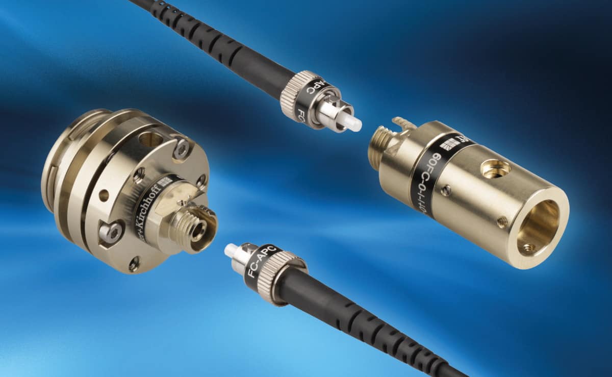
Achromatic fibre couplers offer high efficiency and long-term stability
Schäfter + Kirchhoff offers a series of achromatic fibre couplers and collimators that have been designed to couple multiple wavelengths into single-mode and polarization-maintaining optical fibres. They offer high coupling efficiency, along with excellent pointing stability and long-term stability. All the couplers provide an adjustable focus and support many different types of connector, while amagnetic fibre couplers made from titanium are also available.
High performance: Achromatic fibre couplers from Schäfter + Kirchhoff combine high coupling efficiency with excellent pointing stability. (Courtesy: Schäfter + Kirchhoff)
One part of the product range, the 60SMF series of high-precision fibre couplers has been updated to include ceramic bearings and fine-thread adjustment screws, enabling the focus to be adjusted more easily and more precisely than with previous versions. These devices, which have a diameter of 19.5 mm, have also been optimized to deliver excellent pointing stability as well as the proven long-term stability of earlier devices.
The 60FC-SF series of fibre collimators have also been upgraded to improve the pointing stability and reduce the backlash when setting the focus. These collimators – which can either be used to collimate the radiation emitted from an optical fibre, or in reverse to couple a beam into an optical cable – have now been engineered with a super-fine thread to enable more precise focus setting with a pitch of 0.35 mm.
All the collimators and couplers available from Schäfter + Kirchhoff support focal lengths up to 18 mm, and come with a choice of aspheres, achromats and apochromats. Various anti-reflective coatings are available for wavelengths ranging from the ultraviolet to the infrared.
Schäfter + Kirchhoff was planning to demonstrate its full range of products at both BiOS and Photonics West, but had to cancel last minute due to the surge in COVID-19 cases and the accompanying health risks. Visit the Schäfter + Kirchhoff website to find out more about the company’s products.
The Stamina imaging system from Lambert Instruments provides a comprehensive imaging solution that can be used to record high-speed events in challenging light conditions. Images can be captured, viewed and combined from up to nine different cameras at the same time, and the system can be fully customized to provide greater flexibility as well as easy integration into an existing set-up.
The Stamina system combines advanced hardware with easy-to-use software to form a complete imaging system. The software makes it easy to attach a new camera to the set-up, and supports a wide range of cameras for maximum flexibility. Multiple cameras connected to the system can be viewed and recorded at the same time.
High-speed imaging: The Stamina imaging system from Lambert allows images to be recorded from up to nine separate cameras at the same time. (Courtesy: Lambert)
The system synchronizes the images taken with all of the different cameras, and streams the image data directly to a hard drive to allow images to be captured over long periods of time. Stamina is also supplied with an external Application Programming Interface (API) to enable additional customization and integration.
Visit Lambert Instruments at booth 2067 to find out more about the Stamina imaging system
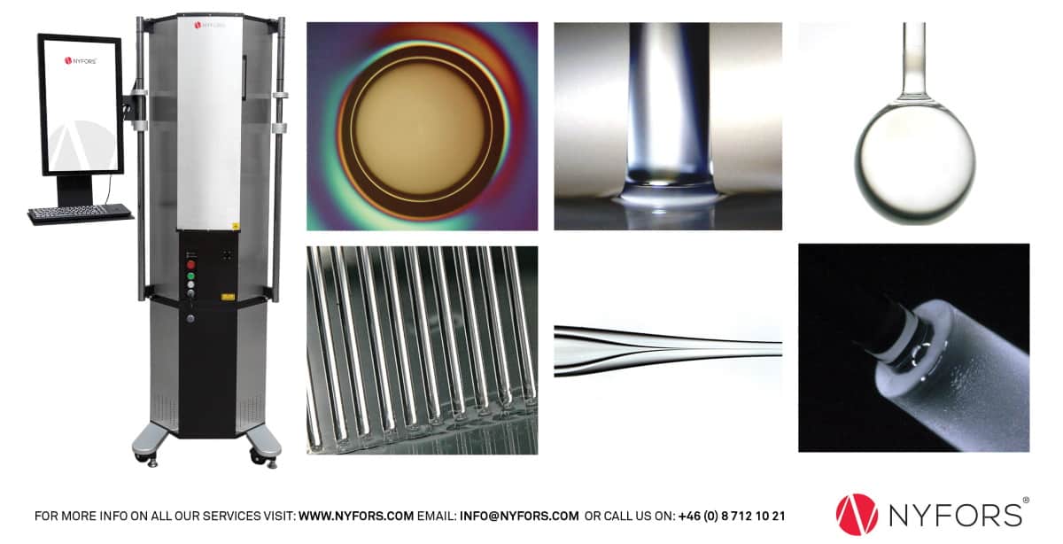
Laser platform offers precision processing of optical components
NYFORS will be showcasing the capabilities of a laser-processing platform that has been designed for the manufacture of high-performance photonics components. The system, called SMARTSPLICER, is a ring-shaped CO2 laser beam that provides precise and contamination-free heating of glass components, making it ideal for tasks such as fusion splicing and glass processing.
In an array splicing process, the platform has been shown to create homogeneous, high-strength splices of 10 fibres or more in a row. High-precision translation stages achieve a placement accuracy of better than ±1 µm, with a spacing between fibres of less than 250 µm.
Laser-processing platform: The SMARTSPLICER platform from NYFORS offers a precise solution for manufacturing high-performance optical components. (Courtesy: NYFORS)
The SMARTSPLICER platform also offers an effective solution for producing ball lenses, with the vertical splicing and ring-shaped heat zone allowing ball lenses with both large and small diameters to be produced with a high degree of homogeneity. “Precise control of the CO₂ laser power, combined with high-accuracy translation stages, offers excellent repeatability and control over the final shape and size of the lenses,” comments Erik Böttcher, CEO of NYFORS.
Outstanding performance has also been achieved when using the platform for splicing gradient-refractive index (GRIN) lenses. “For example, standard fibres can be spliced to the low melting-point, doped glass of GRIN lenses with no component damage,” adds Böttcher. One other unique capability, called linear splicing, allows objects of different sizes and made from dissimilar materials to be joined together with a high-strength and contamination-free bond.
NYFORS will demonstrate the capabilities of the SMARTSPLICER platform at 4.00 pm on Wednesday 26 January (Demo Area 2, Hall D). To find out more, visit the NYFORS team at booth 3201.
Using a novel electronic sensor array, researchers in the US have captured the flow of electrical signals within individual cells, as well as between multiple cells in artificial 3D heart tissue. The minimally invasive device, developed by a team headed up at the University of California, San Diego, revealed a significant difference between the propagation speeds of signals travelling within and between cells. The technique may eventually allow researchers to study and diagnose disorders in vivo in biological tissues.
To fully understand the mechanisms of cell function and disease, it is essential for biologists to measure how electrical signals are conducted: both within individual cells, and between multiple cells in complex tissues. Currently, measurements in individual cells are made using patch clamping, in which currents are generated by applying a controlled voltage across cell membranes. However, this approach is limited by its sensing accuracy, and the scalability of existing technologies makes it extremely challenging to perform on multiple cells simultaneously.
Pop-up sensors: False-coloured scanning electron microscopy of the FET array. (Courtesy: Yue Gu)
First author Yue Gu and colleagues present a more advanced approach in their study, involving a 3D array of highly sensitive field-effect transistors (FETs). These devices are shaped like sharp, pointed tips, and coated with a phospholipid bilayer: the membrane that forms a continuous boundary around all living cells. This allowed the sensors to non-invasively pierce through cell membranes, and detect electrical signals from directly inside.
To fabricate the device, the researchers first cut out the FETs in 2D shapes, then pinned them in specific positions to a pre-stretched elastomer sheet. When the sheet was then loosened, this material then buckled and bent into its final 3D shape.
Unlike previous patch clamping approaches, the team’s FET array could be used to monitor signals from multiple cells at the same time, and even at two different sites within the same cell. This enabled them to measure both the speeds and directions of signals within individual cells, as well as between specific pairs of cells within complex 3D networks.
To test their approach, the researchers studied the propagation of signals within heart muscle cell cultures and engineered 3D cardiac tissues, placed on top of the FET array. For the first time, this allowed them to measure intracellular signals in the 3D tissue. The experiment revealed some particularly intriguing behaviours: showing that electrical signals travel five times faster inside cells than between them.
The result could have broad implications for biologists’ understanding of cellular physiology. By identifying irregularities in signal propagations, the team hopes that clinicians could gain a detailed knowledge of heart disorders such as arrhythmia, heart attack and cardiac fibrosis. Although the practical medical use of the device is still some way off, the approach could eventually lead to FET arrays that can be implanted on real biological tissues, with artificial intelligence processing algorithms employed to offer valuable patient diagnoses.
A surprising property of how resonant photons interact with an absorbing medium has been uncovered by physicists in Canada. They say they have found that even photons passing straight through the medium energize atoms within it, causing atoms to spend nearly as much time in their excited states as those that have absorbed photons. They see their result as a challenge to theorists trying to describe how light interacts with matter quantum mechanically.
Aephraim Steinberg and colleagues at the University of Toronto made the discovery while investigating what happens to a beam of photons passing through a cloud of atoms when the photons’ frequency is equal to that of one of the atomic transitions. Intuitively, they say, it would be expected that those photons exciting atoms within the cloud would be absorbed and then at best re-emitted in a random direction. As such, the flux of photons coming from excited atoms that are detected in the forward direction would be miniscule.
Indeed, they point out, this idea that only absorbed, or “lost”, photons contribute to the excitation springs naturally from theory that tells us the total time atoms spend in the excited state is directly proportional to the number of photons that are lost.
Atomic cloud
To explore this idea further, Steinberg and colleagues have now tied atomic excitations to the detection of individual photons arriving at a detector on the far side of an atomic cloud – to establish whether those photons really contribute nothing to the excitations. They did so not with single photons as such, but instead used single-photon detection to establish when an interacting light pulse’s mean number of photons increases by one.
Their experiment consisted of an ultracold cloud of rubidium-85 atoms stored in a magneto-optical trap and exposed to two counter-propagating laser beams. One of these beams, called the “signal”, was pulsed and resonant with one of rubidium’s transitions, and ended up at a photon detector on the far side of the cloud. The other beam, called the “probe”, was set off-resonance and used to record the phase change associated with atomic excitation. This is possible because the atoms’ ground and excited states having different refractive indices.
The idea was to measure the degree of phase change both with and without a detector click, placing the two sets of results in separate bins. In this way, the researchers could establish for how long the lost and transmitted photons excited the atoms for.
Phase shift
The researchers used signal pulses lasting 10 ns each and emitted a little less than twice a microsecond, with some 60% of the shots being absorbed by the optically-thick medium. By measuring the phase once every 16 ns they were able to distinguish the single pulses’ phase shift from other variations in the medium’s refractive index. They also screened out other sources of noise that could have generated spurious correlations between the phase of the probe beam and the single-photon detector.
As they report in a paper accepted for publication in PRX Quantum and uploaded to the arXiv preprint server, they gathered data for over 100 h and recorded about 6 billion signal pulses. They say they were clearly able to identify the signal pulses’ modulation of the probe’s phase and use their data to compare the phase shift with and without a detector click. Their conclusion is that the phase shift caused by a transmitted photon amounted to 77% of the shift due to an average incident photon.
“The unequivocal implication of this result is that even photons which are ultimately transmitted spend a significant portion of time as atomic excitations,” they write.
Trying to explain their results physically, the researchers say that transmitted photons could naively be expected to excite atoms over longer periods of time than could lost photons – owing to their ability to polarize atoms over the entire length of the sample. But they say that this “egalitarian” model generates physically implausible results for very thin samples.
Photons “switch teams”
They argue instead that “coherent forward emission” – which arises naturally when broadband pulses propagate through an optically thick medium with frequency-dependent absorption – is likely responsible. As Steinberg explains, the phase of a photon’s electric field determines whether the field excites an atom or drives it back down to its ground state. Because broadband pulses develop phase flips, they can start by exciting an atom but then “switch teams” and send the atom back to its ground state before it naturally decays. And when this happens, the released energy is not emitted randomly but instead in the forward direction.
To try and develop a full quantum-mechanical understanding of their latest result, Steinberg and colleagues have teamed up with quantum theorist Howard Wiseman of Griffith University in Australia. They say they have “made a lot of progress” in this direction and are also working on a new round of experiments to test some of the theory’s predictions. This work, they add, will involve varying the atomic cloud’s optical depth as well as the laser bandwidth and pulse shape, in order, as they put it, “to further elucidate the strange history of transmitted photons”.
Commenting on the work, Howard Carmichael of the University of Auckland in New Zealand says that he is not surprised by the result. He explains that an optically thick medium behaving linearly, in which the atoms are close to their ground state, would be expected to absorb incoming resonant photons. In contrast, he argues, a nonlinear medium with most atoms in the excited state would instead be expected to transmit the light. There is, he says, “an implied correlation” between the transmission and the absorber being excited rather than in its ground state.
Steinberg, however, takes issue with this interpretation. “Our absorbers stay close to the ground state yet absorb about half of the incident photons,” he says. “The fact that on occasion we find a transmitted photon certainly does not prove that the absorber was in the excited state.”
Industrial manufacturing is subject to stringent testing protocols aimed at guaranteeing the quality of the final product. In some circumstances, though, these methods are not sensitive enough to detect flaws, leading to incorrect determinations of quality. Researchers at the Istituto Nazionale di Ricerca Metrologica (INRiM) in Torino, Italy have now shown that alternatives based on quantum entanglement can produce more accurate assessments of “good” and “failed” products. Importantly, the INRiM team’s system uses relatively simple equipment, increasing the chances that it could be used in industrial settings.
Some degree of error is inherent even in highly refined procedures such as quality-control tests. Spectroscopic measurements, for example, require a laser source and a detector that are both subject to fluctuations. For tests that need to use low levels of light, as is the case on samples that are highly photosensitive, the signal-to-noise ratio tends to be lower, meaning that it impacts more heavily on the accuracy of the results. In classical methods, the error probabilities depend on the Gaussian distribution of the fluctuations of the entire system – in this case, the laser plus the detector.
In principle, quantum technologies – particularly quantum metrology – offer a way of overcoming the limits of classical systems. Some such technologies are already in use within gravitational wave detectors, where they significantly boost the system’s ability to detect small signals in a noisy background.
Entanglement does the trick
In the latest work, researchers led by Marco Genovese of the INRiM employed a subset of these methods, known as quantum conformance tests (QCTs), to obtain lower error probabilities in the type of measurements used in industrial quality-control assessments. The team’s first step is to entangle photons generated via a process called spontaneous parametric down-conversion, in which pumping a barium borate crystal with a laser at 405 nm produces a special type of entanglement known as two-mode squeezed vacuum states. The entangled photons are then sent down different paths, with one photon passing through the sample being tested and the other following a reference path. The two paths are kept the same length by letting the reference photon pass through a non-absorbing glass. Finally, the photons impinge on different regions of a single CCD detector, which counts photons from each path in order to determine the photon number correlation of the entangled beams.
The team analysed the error probabilities for both classical and quantum correlated methods and concluded that QCT led to better results in all cases. Notably, the researchers demonstrated that this “quantum advantage” persists for a wide range of parameters, even with experimental imperfections. Although the accuracy of the QCT method dropped when they simulated the degree of signal loss expected in a realistic industrial setting, it remained 20% higher than classical methods.
Other use cases
According to Genovese, the experiment demonstrates how QCT can be realized with present technology, making practical applications possible in the near future. He adds that the method could also have other use cases, with one example being “quantum reading” –using entangled photons to read data from a classical memory with greater efficiency than is possible with classical light. “We will pursue the studies of new applications of quantum light to quantum metrology, both exploiting photon number entangled states (as in this case), but also studying other methods [such as] using the properties of colour centres in diamond or by applying new paradigms of quantum measurement (as weak measurements),” he tells Physics World.
Pepijn Pinkse, a researcher at the University of Twente in the Netherlands who was not involved in the work, says that the results are an interesting and novel interpretation of QCT. In his opinion, however, an improvement of 20% is not enough to make the method attractive for widespread use, especially as it requires longer measurement times. “Better results can be obtained by using 10 or even 100 times more light,” he explains.
For that reason, Pinkse thinks that the most likely applications for this technology will be in situations where the light intensity needs to be kept low, such as in tests of photosensitive systems such as biological tissues or pigments that can bleach. He also suggests that bigger gains in accuracy might be obtained by extracting data from correlations in other quantities, such as the polarization of the entangled photons.