Cracking the quantum code

Science writer Philip Ball joins Kate Gardner and Tushna Commissariat from Physics World to discuss the TV thriller Devs. Listen to the full conversation in the Physics World Weekly podcast.

To understand quantum physics – as far as anyone does – requires a lot of imagination, and a fair bit of philosophy. If you examine whether, say, the Many Worlds interpretation is correct, that opens up discussions of determinism versus free choice. Indeed, proving which quantum physics interpretation is true could have huge implications for humanity, and for how we live our lives. While we may not quite be there in real life, that is what the characters in new TV show Devs are attempting to unravel.

This sci-fi thriller from writer-director Alex Garland (28 Days Later, Ex-Machina) has quantum physics at its heart and truly embraces all the complexity that entails. The screen is often packed with smart people debating the nature of reality – and yet all eight episodes are also action-packed and thrilling. In the opening scene of Devs, a young couple sit in their kitchen having a conversation about quantum cryptography over breakfast. What I really appreciated was that this dialogue is neither plot explanation, nor mere technobabble. It’s establishing two scientists having a realistic technical discussion – a friendly disagreement – about their work.

The woman in this cosy set-up is Lily (played by Sonoya Mizuno), a quantum-communications expert. Her boyfriend is Sergei (Karl Glusman), an AI developer. They both work at Amaya – a quantum tech company on the outskirts of San Francisco run by its enigmatic founder Forest (Nick Offerman). Amaya is a large company with a beautiful campus – including a small woodland that disguises the location of the super-secret Devs building. Everyone at Amaya knows this department exists, but only those who work in Devs know what it does.

To reveal exactly what this clandestine department does – and how – would certainly constitute a spoiler, but the building itself is worthy of comment. From the outside it is a giant concrete bunker. Inside it is the one thing in this series that I could find fault with. A glass and steel computing lab is suspended magnetically at its centre, surrounded by a vacuum moat, several metres wide, separating it from the outer walls, floor and ceiling. The only access is via a horizontal lift that traverses the vacuum. No electronic devices – or cleaners – are allowed in, but there is somehow a fully functioning bathroom inside. I couldn’t help but wonder how exactly the plumbing functions.

Google’s Quantum AI Lab was a major inspiration in this show’s design

Nitpicking aside, this piece of futuristic architecture is built around a quantum computer – not the black box of press releases from D-Wave Systems, but a device made of tubes and copper coils resembling more than anything else an old carriage clock, with not a circuit board in sight. It’s not a million miles from press images of Google’s quantum computers – not the only time Google was a major inspiration in this show’s design.

Lily is our hero, a practical and capable woman whose life is thrown into disarray when Sergei is transferred to Devs. Through him we meet the rest of Devs team, led by the severe chief designer Katie (Alison Pill). They are all odd in their way, but these are not cardboard mockeries. The only “type” under fire here is Forest as the tech CEO, whose financial success has given him power and control over people.

Sonoya Mizuno in Devs

Mizuno, a Japanese-British ballet dancer and actor, has worked with Garland twice before (you may remember her as Kyoko, the attendant in Ex-Machina). She is utterly convincing as Lily, even while – like almost all characters in this drama – keeping the audience guessing as to what side she is on and how much of what she says is true. She is shown a little more often than is necessary in her underwear, but in that outfit, she reminded me of Ripley in Aliens, which is a strong point of reference.

Offerman is similarly an inspired choice to play Forest. He is best known for playing gruff but loveable Ron Swanson in the TV show Parks and Recreation. As Forest, there are moments of that same leadership figure: affable and brusque in a charming way, but he can turn on a pin to something much more sinister. Which makes Devs, his pet project, equally menacing.

It should come as no surprise that a project from Garland is well acted and beautifully shot, but I will say that the science component of his fiction has come a long way from the dubious physics of Sunshine, his 2007 film about reigniting the Sun, which is prematurely dying. That film boasted one Brian Cox as its scientific adviser, while Devs was developed in conversation with a whole raft of people knowledgeable about quantum – including Google’s Quantum AI Lab.

Garland and Mizuno personally visited the Google lab, and this visit – along with several others to a host of Silicon Valley companies – is evident in the set design and the way people move around it. Aside from the supremely unnerving giant statue at its centre, the architecture at Amaya is wonderful. A friend described the architecture as “realistic and tech-bro”, but I think that is misleading, because there is nothing “bro” about this series. Perhaps that’s a little idealism on Garland’s part, or perhaps that’s the Silicon Valley he saw during his research.

If you’re looking for an entertaining 360 minutes that explores cause and effect, or the true meaning of determinism, but is also an absorbing thrill ride, Devs is just the ticket.

Working in medical physics: not your average career

For certain fields of physics, it can be tough to explain how the research has a direct benefit to society. That is never the case with medical physics – a career where you can apply a technical skillset to directly improve people’s everyday lives. In this episode of the Physics World Stories podcast, Andrew Glester catches up with three medical physicists from The Christie – the largest cancer hospital in Europe – to learn about their careers.

Heather Williams, the principal physicist in nuclear medicine at The Christie, speaks about some of the latest developments in positron emission tomography (PET). Williams also explains how the COVID-19 pandemic has affected the working practices at the hospital, requiring some difficult decisions around risk management. Among other developments, clinical engineers have been working with industry to develop new systems to deliver oxygen to coronavirus patients.

Later in the podcast, you will also hear from Patricia Amata who is studying for a PhD in ultrasound modalities. Medical ultrasound is most commonly associated with the field of obstetrics, where it is used to generate images of the foetus developing in the womb. But this non-ionising form of imaging is used across the medical spectrum – from breast scans to neurology, and often as a way of calibrating other imaging techniques.

Finally, clinical scientist Imran Patel speaks about the Christie’s proton therapy centre, which has been treating patients since December 2018. Patel, who leads the proton therapy physics group, explains why proton therapy can offer benefits in certain circumstances, such as paediatric cases. Unlike photons and electrons, protons beams can deliver a radiation to a highly localized sites, minimising damage to surrounding healthy tissue.

You can take a look inside the Christie’s proton therapy centre in this video produced in 2019.

Calculating the speed of coronal mass ejections could avoid unneeded satellite shutdown

Satellite operators could be doing more harm than good by shutting down their systems whenever a coronal mass ejection (CME) from the Sun is forecast to arrive at Earth, UK researchers have suggested. Mathew Owens, Mike Lockwood and Luke Barnard at the University of Reading show that the speeds and magnetic field intensities of the bursts could be just as important to consider as their arrival times when deciding when to turn satellite systems off. If applied, their ideas could significantly improve the efficiency of many satellite operations.

Originating from the Sun’s dynamic surface, CMEs are high energy bursts of plasma that travel through interplanetary space, accompanied by strong magnetic fields. When they interact with Earth’s atmosphere, they can trigger solar storms that cause severe damage to satellite systems if they are operating at the time. To predict these disruptions, astronomers measure the speed at which CMEs travel through space to make accurate forecasts of when they will arrive at Earth.

Currently, many satellite operators adopt a “better safe than sorry” approach when responding to these forecasts. Whenever a CME is predicted to arrive, they will completely shut down their systems to avoid any damage. However, the Reading trio argue that these current early warning systems do not account for a simple yet crucial fact: while all solar storms are triggered by CMEs, not all CMEs cause in damaging events.

Many false alarms

The researchers believe that this oversight is now causing many false alarms, forcing satellites to shut down when they can be operated safely. Furthermore, the cost of unneeded shutdowns could be even greater than the cost associated with solar storm damage. To improve the response to CMEs, the team suggest that alongside arrival times, it is just as important for CME forecasts to incorporate information about their speeds, and the intensities of their accompanying magnetic fields – both key indicators of solar storm severity.

Owens and colleagues tested this principle through a simple analysis of solar wind data, in which they calculated the costs of shutting down satellite systems only when CME speed and magnetic field measurements indicated that damaging weather was about to occur. Compared with more frequent shutdowns which only considered CME arrival times, they found that the resulting costs were significantly reduced.

By quantifying the costs of false alarms in this way, the team’s findings could inform more sophisticated approaches to mitigating the damage of solar storms in the future. If adopted more widely, their approach could help to streamline the efficiency of satellite operations; significantly reducing costs incurred by the many groups which rely on them.

The research is described in Space Weather.

The secrets of success in electron and ion optics

Vocation, collaboration and innovation provide a unifying frame of reference for the physicists and engineers of Kimball Physics, a New Hampshire-based technology company that specializes in the design and manufacture of precision electron sources, electron optics and ultrahigh-vacuum (UHV) chambers and components. That frame of reference, it seems, is as solid today as it was 50 years ago, when physics professor Chuck Crawford spun Kimball Physics out from his research programme at Massachusetts Institute of Technology (MIT).

Consistency matters to Crawford, which is why the goal back then remains the mission at Kimball Physics today: “To advance humankind by doing good physics – specifically electron optics and vacuum physics – and all the while growing, being good citizens, making a living, and having fun.” Context aside, Crawford’s commercial vision was to identify an opportunity to advance the field of UHV electron and ion optics, and specifically the niche where Kimball Physics could add most value for a range of customers – from university researchers and US national laboratories to multinational “big-science” facilities and semiconductor industry OEMs.

On that canvas, Kimball Physics has carved out – and subsequently scaled – its specialist niche to encompass the design and manufacture of electron optical equipment for the semiconductor industry; electron sources for electron microscopes and electron lithography; as well as custom high-brightness sources and related technologies for free-electron lasers, particle accelerators and X-ray systems. That custom offering includes a mix of products tailored for the exacting requirements of the space industry as well as specialist Multi CF vacuum chambers for “cold physics” research and other exotic physics experiments.

Employee focus meets customer focus

Remarkably, five decades after starting the business, Crawford remains engaged with the operations at Kimball Physics. “Chuck is still in regular communication and I doubt he will ever stop thinking up new ideas,” explains Abigail LePage, a physicist and Kimball Physics’ president and chief executive officer. “He doesn’t consider what he does as work. He’s having fun and that mindset informs the collective culture here at Kimball Physics.”

That culture is further defined by “open-book management”, a non-hierarchical working model that seeks to empower all staff by treating them as partners in the business. Transparency is the key, ensuring Kimball Physics’ teams have a holistic view of the company’s financial metrics – revenue, profit, cash flow, capital expenditure and the like – so that they can make informed decisions to drive operational and strategic priorities.

That trust in the workforce yields significant gains – and not just commercially. “Many of our staff see what they do as more of a vocation,” claims David Altobelli, senior scientist at Kimball Physics. “Everybody takes a lot of pride in their work and pushing the technology forward.”

“No” is not an option for physicists when an important project must move forward. Necessity is the driver of innovation

David Altobelli, senior scientist at Kimball Physics

If vocation underpins the work ethic among Kimball Physics’ scientists and engineers, the vendor’s overarching commercial drivers are shaped by a collective focus on new product innovation and an open, inclusive dialogue with customers large and small. “Innovation at Kimball Physics is all about assimilation,” says Altobelli. “Tracking the pulse of the market requires close collaboration with scientific and industry customers to ensure that our product development aligns with their research and commercial priorities.”

Kimball Physics LePage

As such, about 30% of the products that Kimball Physics ships each year are custom-made to users’ bespoke technical requirements. “We’re motivated by the challenging problems and opportunities that we see in the custom business,” Altobelli adds. “After all, today’s one-off product, for a single end-user, can evolve into tomorrow’s standard product for many.”

Unsurprisingly, Kimball Physics is active along many R&D coordinates – in each case working closely with customers. NASA is a case in point. More than 10 years ago, well before additive manufacturing became a mainstream technology, the vendor teamed up with colleagues at the US space agency to build a platform for electron-beam free-form fabrication – an innovation that may ultimately enable additive manufacturing in space. Other NASA projects involve laboratory testing and characterization of satellite shielding materials – essentially using electron and ion sources to simulate the solar wind that a craft will experience – as well as specific product innovations to minimize power consumption and footprint (e.g. delivering a 50 μA electron-beam source for satellite positioning that consumes <100 mW).

“We do take risks – within reason – and are prepared to back projects that some vendors would walk away from,” explains LePage, citing Kimball Physics’ work on the optics for novel electron sources such as superconducting quantum dots, cold electron sources and laser-excited emitters. “These more speculative plays are crucial in loading our toolbox for future product innovations,” she adds.

High-value vacuum innovation

Another promising commercial opportunity is ultrafast electron microscopy, with Kimball Physics supplying electron sources and column optics to research groups for a new generation of microscopes that offer temporal resolutions in the sub-nanosecond regime for single-shot applications (with up to 10 million electrons/pulse) and into the deep femtosecond range for stroboscopic applications (with thousands of electrons/pulse).

Elsewhere, the firm’s Multi CF UHV chambers and associated hardware – “the result of inadequately supervised physicists running amuck with CNC machines”, according to Crawford – provide a core enabling technology in cold-atom physics experiments, where accuracy of port alignment is critical for optimal laser access. A high-profile collaboration with NASA’s Cold Atom Lab, for example, has seen the Kimball Physics Multi-CF “mini” cube UHV chamber deployed on the International Space Station to support such studies. Other Multi CF applications include electron gun and ion source housings; detector housings and subsystems; as well as portable, low-cost UHV chambers.

“Our Multi CF chambers enable UHV operation with enhanced capabilities – more of a ‘value-added’ system or instrument housing than just an evacuated environment,” claims Altobelli. What he’s referring to is an array of unique Multi CF sizes and configurations, featuring precise geometries for optimized internal access, highly polished surfaces, contoured interiors and minimal welds, and annular grooves around most ports to allow mounting of internal hardware and devices. Equally, while most of the standard Multi CF chambers and fittings are made from monolithic structures of 316L stainless steel, customized options are also available in titanium for more demanding technical requirements (such as reduction of hydrogen outgassing, local magnetic effects and weight).

Looking ahead, a significant chunk of Kimball Physics’ long-range R&D effort will focus on realizing next-generation electron sources and optimized optics to address the already large (and growing) markets for electron-beam inspection, metrology and electron lithography within the semiconductor industry. “Electron emitters with precision optics are our dominant product line and key for our future product innovation,” notes LePage.

Of more immediate concern to LePage and colleagues is mapping a course through the current Covid-19 disruption, ensuring Kimball Physics continues to remain on a firm footing as it looks to the next 50 years. “We’re proud of being an innovative and solid high-tech company,” she concludes, “and we don’t intend to let the pandemic change that.”

Radiation alters ceramic grain boundaries

Grain boundaries in ceramics may not be as chemically stable as previously thought. So say researchers at the University of Wisconsin-Madison in the US who have found that carbon atoms collect or segregate at the boundaries of silicon carbide – a technologically important ceramic – when the material is exposed to ionizing radiation. The result could help improve our understanding of ceramics in general and aid the development of better ceramic materials for applications in nuclear energy.

Changes in the chemical composition of grain boundaries – the interface between two different grains in a polycrystalline material – can dramatically affect a material’s mechanical strength, corrosion resistance and radiation tolerance. This is because the boundaries act as traps for defects, sites for corrosion reactions and channels for diffusing other chemicals through the material.

Radiation-induced segregation

Radiation-induced segregation is a well-known phenomenon in metal alloys. When such alloys are irradiated, the bombardment of neutrons, ions and other particles creates defects. More specifically, defects known as Frenkel pairs form when an atom leaves its place in the crystal lattice (creating a vacancy) and lodges in a nearby location (becoming an interstitial). Frenkel pairs can then either recombine with each other or migrate to defect traps such as grain boundaries. If different types of atoms in the alloy move at different rates, certain elements build up or become depleted in the vicinity of the boundaries.

Because ceramics have stronger interatomic bonds than metals, researchers had long assumed that the atoms in ceramics were not subject to this type of segregation. Now, however, a team of researchers led by Izabela Szlufarska has turned this idea on its head by studying the behaviour of grain boundaries in silicon carbide (SiC). This ceramic is employed in nuclear energy and jet engines, among other high-tech applications, and it also shows promise for advanced nuclear reactors and microelectrochemical systems operating in harsh conditions.

Szlufarska and colleagues found that the material’s grain boundaries became enriched with carbon atoms when they bombarded it with ions at a temperature of 300°C. At this temperature, which is much lower than is required to initiate radiation-induced segregation in metals, they found that the radiation dislodged some carbon atoms from their normal lattice sites. Just as in metals, the resulting pair of defects in the SiC included a vacancy site and an interstitial (in this case, a loosely-bound carbon atom). They also observed that these untethered interstitials migrated towards the grain boundaries, where they accumulated, changing the material’s chemistry. The degree of segregation diminished when they irradiated the material at 600°C.

Radiation as a tool to fine-tune chemistry

The researchers obtained their result by analysing the chemical composition of grain boundaries in pristine samples of SiC grown by chemical vapour deposition using the latest scanning transmission electron microscopy techniques at UW Madison and Oak Ridge National Laboratory. They say that the phenomenon is likely to occur in other polycrystalline ceramics, too, and they also note that the segregation might be turned into an advantage, by making it possible to produce new types of ceramic materials with improved properties. “The radiation might in fact be used as a tool to fine-tune grain boundary chemistry,” explains study co-author Xing Wang.

However, the researchers, who report their findings in Nature Materials, also note that the much lower temperatures for carbon enrichment in SiC suggest that our understanding of radiation-induced segregation in metals may not transfer directly to ceramics.

“Unlike metal alloys, ceramics have much more complex energy landscapes for defect reactions and multiple sublattices in which defects can migrate,” they say. To explore this landscape, the team developed an ab initio informed rate theory model that reproduces and explains the low-temperature radiation-induced segregation behaviour in SiC. These calculations also suggest that carbon segregation near grain boundaries in SiC comes about due to two factors: the different diffusivities of vacancies and interstitial defects; and the different reaction energy barriers between silicon and carbon sublattices in the material.

In their future studies, Szlufarska and colleagues plan to study how radiation-induced segregation in SiC depends on other conditions – for example, the total dose of radiation. They will also investigate different types of grain boundaries.

Contraceptive hydrogel proves safe in rats

Researchers from India have developed a biodegradable gel for female contraception.  Reporting their results in Materials Science & Engineering C, they found that the active ingredient styrene maleic anhydride (SMA) embedded in a biodegradable hydrogel kills sperm and prevents egg cell formation. Implanting the gel in female rats showed excellent bio-compatibility, paving the way for creation of a non-hormonal contraceptive implant. Such a gel would expand the hormonal and non-hormonal contraceptive options currently available for women, many of which cause side effects.

Potential for a non-hormonal female contraceptive

SMA is already in Phase III clinical trials as a male contraceptive implant in the vas deferens, the vessel transporting sperm in men. But in addition to killing sperm, SMA also disrupts the development of female egg cells. The astonishing combination of these two effects led the research team headed by Piyali Basak and Sujoy Guha to design a female version of the gel.

To achieve long-term dosing, their team wanted to incorporate SMA into a gel that would be inserted in the uterus, the female reproductive organ that nurtures the developing foetus till birth. A suitable gel has to be safe for the body, biodegradable and allow the incorporation of SMA without inactivating the drug.

To create such a gel, polycaprolactone (PCL) proved to be a good starting point. It is commonly used for medical applications as a biodegradable polymer; however, it is not flexible enough for this application. To achieve the required flexibility, the researchers mixed PCL with PEG (polyethylene glycol) and polymerized them as diacrylates (DA). The polymers were fabricated into a PCL-DA:PEG-DA hydrogel, a water-based gel made from an insoluble polymer. They then added five different concentrations of SMA and characterized the resulting gels.

Selecting the best concentration

First author Bhuvaneshwaran Subramanian and his team tested the physical properties and biodegradability of the gels, as well as the influence of exposure to ethanol, varying temperature and mechanical stress.

Research team

Out of the five samples with different SMA concentrations, the team further evaluated the three most promising ones using sperm and rat uterine cells. As intended, the gel killed sperm but did not harm the uterine cells. The sample with the highest spermicidal activity was then chosen for implantation in a rat.

Because rats do not have a true uterus, the researchers implanted the hydrogel in the fallopian tubes, which serve as a model for the human uterus. The implanted gel had no effect on any of the tested tissues or organs and degraded after 150 days. Blood analysis revealed no signs of inflammation, toxicological symptoms or metabolic and hormonal changes.

These findings suggest that the SMA hydrogel should be safe for implantation in the female reproductive organs. The next step will be to investigate whether the combination of SMA and the PCL-DA:PEG-DA hydrogel also works as an effective contraceptive when implanted in rats.

Colour-changing probe maps stresses in soft materials

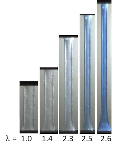
images of elongation test

Directly measuring stresses in soft materials as they deform is no easy task, but a team of researchers in France and the US have now developed a colour-changing force-responsive probe that can do just that. The device, which is based on a force-sensitive molecule embedded in an elastic polymer (elastomer) network, can be used to build up a quantitative map of internal forces in a structure by optical means alone.

When a mechanical load is applied to an irregularly shaped object, the stresses and strains it produces will also be irregular. Measuring these internal forces is important for predicting where the object will break, but because soft materials often deform considerably before they fail, such measurements are particularly difficult to make.

At present, only a few techniques can directly measure stresses in soft materials. The most common method is to measure strains and then perform a mathematical simulation to calculate the corresponding stresses. Such calculations are, however, known to be unreliable for large strains and strong strain gradients.

Force-sensitive molecules

In recent years, researchers have been exploring ways of making stress sensors out of force-sensitive molecules incorporated into polymers. When these “mechanophore” molecules are activated by a force of a sufficient size, they undergo chemical reactions that cause their optical properties (such as fluorescence, luminescence and colour) to change.

One commonly used mechanophore is an organic compound known as a spiropyran. When a spiropyran-containing polymer network deforms, the forces on the bonds of this molecule cause it to transform into a chemical variant called merocyanine that absorbs visible light. By shining a light on the sample and monitoring its change in colour from transparent to blue, researchers can therefore directly measure the fraction of molecules that have undergone the chemical reaction. This, in turn, gives them a measure of the average stress applied on the material at the point at which the colour change is observed.

Mechanochemistry

“This field of study is called mechanochemistry – that is, chemistry triggered by mechanics,” explains Costantino Creton from the ESPCI in Paris, who led the new research effort. “It opens many possibilities for measuring internal forces using optical visualization techniques alone.”

Going from qualitative colour-change detection to quantitative mapping of heterogenous stress fields is not as easy as it sounds, however. For one, Creton and colleagues note that the spiropyran must be randomly and homogenously incorporated into the material being tested. The average force produced on the molecule must also be directly related to macroscopic stress applied, and the molecular sensor should activate before the material breaks.

A calibration curve

The researchers tested their technique on two elastomer materials with very different hardening properties. They began by incorporating spiropyran into these materials as a cross-linker and tracked the colour change of the molecule as they applied tension to the samples along a single axis. By varying the concentration of the spiropyran within the network of the elastomers, they produced a calibration curve of applied stress versus colour change. They then used this stress-colour curve to determine the stress distribution around pre-existing cracks within the samples. This stress distribution would be much more difficult to obtain using conventional techniques, as mentioned, since the materials host strong localized stress gradients.

Afterwards, the team, which also includes researchers from the University of Colorado at Boulder, compared the experimental stress fields with theoretical simulations of the same materials. The optical measurement exactly matched these calculations, thus validating the method, Creton says.

This internal probe technique, which is detailed in Science Advances, could be used to test statistical fracture modelling of soft, tough materials and more generally to quantify stresses in irregularly shaped objects from simple optical observations with a (red-green-blue) camera, he adds.

The researchers say they would now like to try out their approach on composite materials with a wider range of applications. “We would also like to test metamaterials, which have very heterogenous internal structures and complex mechanical behaviours,” Creton tells Physics World. These materials are artificially engineered compounds with properties such as a negative Poisson ratio that are rare or absent in natural materials.

Quantum dot solar cells get greener

Semiconducting nanocrystals called colloidal quantum dots (CQDs) are ideal for applications such as large-panel displays and photovoltaic cells thanks to their high efficiency and colour purity. Their main drawback is their toxicity, since they have traditionally been made from cadmium or other heavy metals, such as lead. Researchers at the Los Alamos National Laboratory in the US have now engineered cadmium-free QD solar cells that reach efficiencies on par with those of their environmentally-unfriendly counterparts. The key to the new devices’ high performance is their tolerance to defects, they say.

CQDs can be synthesized in solution, which means that films of these nanocrystals can be deposited quickly and easily on a range of flexible or rigid substrates – just like paint or ink. Such semiconducting nanocrystals are ideal for making highly-efficient inorganic solar cells that emit light via a process known as radiative recombination. Here, an electron in the valency energy band in the QD absorbs a photon and moves to the conduction band, leaving behind an electron vacancy, or hole. The excited electron and hole then recombine, releasing a photon.

The advantage of using CQDs as photovoltaic materials in solar cells is that they absorb light over a broad spectrum of solar radiation wavelengths. This is because the band gap of a CQD can be tuned over a large energy range by simply changing the size of the nanocrystals. Such a size-tuneable property has allowed the efficiencies of these QDs to rapidly approach those of traditional thin-film photovoltaics, such as PbS, CdTe and Pb-halide perovskite QDs.

Free from toxic elements

A team of researchers led by Victor Klimov have now developed high-efficiency QD solar cells that are free from any toxic elements. They made their new devices by reacting copper, indium and selenium and then adding zinc to the mix to produce zinc-doped QDs. They then incorporated these QDs into voids of a highly porous titanium dioxide (TiO2) film, which plays the part of a charge-collecting electrode. The electrode was immersed in a Na2S electrolyte.

When the QDs in the device absorb incoming photons from sunlight, tightly bound electrons in the valence band get excited into a high-mobility conduction band. These electrons subsequently migrate to the TiO2 electrode, generating a current in the process.

The researchers say they were “pleasantly surprised” by the results of photovoltaic and spectroscopic measurements on the new devices. Because their QDs have a very complex composition – four elements are combined in the same nanosized particle – they are prone to (intragap) defects, Klimov explains. These defects act as traps in which electrons get stuck, which means that electrons and holes have time to recombine instead of being whisked apart to produce useful current.

“However, despite these imperfections, the ZCISe QDs showed near perfect performance in the new solar cells,” says Klimov. “Per each 100 absorbed photons, we detected 85 photogenerated electrons, implying that the photon-to-electron conversion efficiency was 85%.”

Defect-mediated photoconversion

According to the Los Alamos team, who report their work in Nature Energy, the defects in their material actually help the photoconversion process along, rather than impeding it. In particular, the material’s high photovoltaic efficiency stems from a peculiar mechanism involving two types of intragap defects, they explain. The first, identified as shallow surface-located electron traps, enhance electron transfer between the QDs and TiO2 electrode. The second, identified as Cu1+ hole-trapping defects, help transfer holes between the QDs and the electrolyte.

The traditional assumption that surface defects are always detrimental thus does not seem to hold true for ZCISe QDs, they say. Indeed, the structures may even be protecting electrons and holes from unwanted recombination. This implies that surface traps are electronically coupled to the TiO2 electrode and, importantly, that the energy of these traps is high enough for electrons to transfer efficiently into the TiO2 conduction band.

The high photoconversion efficiencies, combined with the remarkable defect tolerance and toxic-element-free composition of these QDs makes them promising materials for a commercially viable solar-cell technology, they conclude.

Electron accelerator recycles energy

Physicists usually have no shortage of plans to build very expensive particle accelerators – but some researchers are working to make accelerator technology cheaper, and one way is to recycle much of the energy initially used to accelerate particles. A collaboration in the US has now shown it can successfully operate such an “energy recovery linac” by combining superconducting cavities with precisely designed permanent magnets.

The synchrotron has long been a popular way of accelerating electrons and other charged particles. Energy is transferred to bunches of charged particles by sending them through a series of radiofrequency cavities while magnets keep them on a circular path for thousands of orbits. These machines are widely used both as high-energy colliders and as sources of very bright X-rays for a wide range of science.

While this cyclic acceleration produces very high average powers, the bunches of particles will gradually spread out and lose intensity as well as polarization. As a result, linear accelerators (linacs) are used to create the brightest particle beams. These fire particles in a single shot along a straight section of cavities, yielding bunches with very high energies and exceptional intensities. But these machines also have a downside – they consume a huge amount of energy per shot, which limits their firing rate.

Best of both worlds

Energy recovery linacs (ERLs) are designed to combine the best of both worlds. These devices send electrons through a linac and then guide them around a circuit back to the accelerator entrance – with just a few having had their energy tapped along the way. This process takes place N times, with the particles gaining energy on each turn. Then the logic is reversed, thanks to a shift in the electrons’ path length of half a cavity wavelength. The particles travel another N times around the circuit, but rather than absorbing additional energy from the cavities they instead give it back. Once their turns are complete and they have shed all the energy they originally acquired, they are dumped.

With most of this energy transferred to other electrons subsequently injected into the circuit, which themselves go through the same 2N cycles, an ERL can accelerate a given number of particles using a small fraction of the energy consumed by the equivalent linac. In principle, this allows such a device either to generate much higher luminosities from a given electricity budget, or to consume less power for a given luminosity. While the latter option would reduce operating costs, both should lower construction costs – given that linac cavities are more expensive to build than the magnets used to steer electrons.

The idea is not new, having been put forward originally by Maury Tigner at Cornell University in the US in 1965. However, the scheme had to overcome a number of hurdles in the intervening decades. One has been developing the superconducting cavities that make linacs more energy-efficient. Another challenge has been merging beams at the linac entrance and separating them at its exit, as well as dealing with the higher-order modes inside cavities that can cause particle bunches to break up. Difficulties notwithstanding, the scheme has been put into practice at several locations including Novosibirsk State University in Russia, which operated a copper-cavity ERL with multiple turns (N=4) for the first time.

Multiple passes

The latest work, carried out by Georg Hoffstaetter of Cornell University and colleagues, makes progress by instead demonstrating multiple passes using a superconducting linac. The Cornell Brookhaven Energy-Recovery-Linac Test Accelerator (CBETA) has been built and tested at Cornell but relies on magnets developed by Dejan Trbojevic and team at Brookhaven National Laboratory. These are quite different to the electromagnets used in synchrotrons, whose fields ramp up to prevent electrons from flying out of the machine as they pick up speed — but cannot accommodate electrons with different energies. Instead, the CBETA magnets generate a field shaped so that it can simultaneously guide eight sets of electrons, with four different energies, around the circuit back to the linac. Being permanent, rather than electromagnetic, these “fixed-field alternating-gradient” magnets provide an additional energy-saving feature over traditional linacs.

Hoffstaetter and colleagues carried out the first test of CBETA in June last year, showing that the machine could recuperate 99.8% of its input energy after accelerating and decelerating electrons in single passes. Then just before Christmas, the researchers demonstrated the full complement of eight passes. As they report in a paper accepted for publication in Physical Review Letters, they took electrons 6 MeV kinetic energy and stepped their energy up to 42, 78, 114 and 150 MeV, before stepping the energy down so that it ended up back at 6 MeV.

The researchers say that the CBETA technology could be used in a variety of applications including medical isotope production, cancer therapy or in the manufacture of microchips. It has also been designed to show how to “cool” ions that will be collided in the $2bn Electron-Ion Collider approved for construction at the Brookhaven lab in January. Designed to probe the composition of protons and neutrons with unprecedented precision, the collider relies on minimizing particles’ energy to maximize collision rates.

Having shown that CBETA can work in principle, Hoffstaetter and colleagues are now working to boost its performance. To protect equipment and personnel, they restricted the machine’s current on the December run to just a few nanoamps. But they now want to raise that towards a target of 40 mA. “A push to high current will be the next stage of this accelerator,” they write.

Two new frequency combs could boost telecoms and molecular fingerprinting

Frequency combs are one of the most important developments in metrology in the 21st century, but conventional combs are bulky and highly sensitive to external perturbations. Now two independent groups present key developments in solid state frequency combs that could lead to robust, convenient combs for use outside the laboratory. The first is an integrated, telecommunications-wavelength comb that stabilizes itself every time it is turned on. The second uses a completely new mechanism to generate frequency comb emission in the mid-infrared – a region crucial for molecular spectroscopy.

Frequency combs are pulsed lasers often described as rulers of light because they produce extremely short pulses that comprise light at regularly spaced frequencies. By fixing one of these frequencies very precisely – for example using an atomic clock – one can measure the frequency of a light signal by studying how far along the comb it falls from this reference frequency. Frequency combs have proved immensely useful in the laboratory for building better atomic clocks, improving time and frequency standards and also doing ultracold atomic and molecular spectroscopy.

The use of traditional frequency combs, however, is constrained by their need for high-power, ultrastable lasers, amplifiers and other components such as isolators to prevent feedback from destabilizing the laser. In the past decade or so, researchers have sought more user-friendly devices for applications such as fibre-optic multiplexing, time-keeping and molecular detection.

Simple components

In 2018, researchers at Columbia University in New York City led by Michal Lipson and Alexander Gaeta unveiled a solid-state, telecoms-compatible frequency comb that eliminated many specialist components. It used a low-power, electrically-pumped semiconductor laser. When a solid-state microresonator was injected with light at 1579 nm wavelength, Kerr non-linearity caused sidebands to appear at precisely spaced frequencies. The proportion of the energy in these modes gradually increased, forming a frequency comb.

Although this was a huge breakthrough, there were difficulties. A complex process was required to achieve and maintain the comb operation, and even then it did not reliably produce phase- and intensity-stable pulses called solitons. “If it’s not producing solitons, it’s not a quiet comb”, explains John Bowers of the University of California, Santa Barbara, “If you want to make an atomic clock, or a lidar, or a wavelength division multiplexing transmission system, you don’t want modulation instability. It’s not useful for most applications.”

Now, Santa Barbara researchers led by Bowers, together with scientists at Caltech and EPFL in Switzerland, unveil an integrated, solid-state laser that solves these problems. Whereas traditional frequency combs need to prevent feedback between a microresonator and the laser, this latest design utilized feedback.

Much lower noise

A cheap semiconductor laser called a distributed feedback (DFB) laser was integrated into a chip that was placed a small, precisely-controlled distance from a microresonator mounted on another chip. A physically complex non-linear interaction between the laser cavity and the microresonator created a very simple result: every time the laser was switched on, the microresonator automatically tuned itself to produce solitons. Remarkably, the resulting frequency comb had orders of magnitude lower noise than the original laser: “DFB lasers are crappy,” says Bowers, “People pay $60,000 for a laser to get linewidths that aren’t as good as this.” Moreover, the soliton state tolerated environmental disturbances such as temperature fluctuations.

The researchers hope their device could make frequency combs much more widespread: “We believe we can very soon integrate this all onto a single chip,” says Bowers. “It could be a millimetre long, it could be mass produced, it could be quite cheap, and it wouldn’t take a PhD to run. That’s what’s exciting about this.”

Turnkey system

Gaeta is impressed: “You can argue that microresonator combs have been the most active field in non-linear photonics in the past decade,” he says. “My work with Michal Lipson was the first real integrated system and these guys have made an another important step in further integrating it and making the system ‘turnkey’. It’s an important advance in taking this technology into the field.”

Meanwhile at Harvard University, Federico Capasso and colleagues focussed on creating frequency combs that operate in the mid-infrared region at 2.5-10 µm wavelength – a part of the electromagnetic spectrum in which molecules have unique spectral fingerprints. While quantum cascade lasers (QCLs) are readily available in this region, turning them into frequency combs has proven very difficult.

Surprising result

 Capasso’s team investigated the possibility of producing a mid-infrared frequency comb from a quantum cascade ring laser, which behaves as its own microresonator when electrically injected. Traditional QCL frequency combs rely on bar-shaped cavities to create standing waves – something that does not happen in a symmetric ring cavity. So, the researchers added a defect to the ring to break this symmetry and allow standing waves to form. “Purely as controls, we put a few perfect rings on the chip,” explains Harvard’s Marco Piccardo. “To our surprise, these were also forming frequency combs…This is where we started scratching our heads.”

After much theoretical analysis of the laser physics, the researchers realized that the explanation lay in an instability in a non-linear differential equation called the complex Ginzburg-Landau equation, which describes spatially extended systems of coupled non-linear oscillators: “It’s not observed in bars,” says Piccardo, “The fact that a ring laser can go into this frequency comb regime is a new type of turbulent instability for quantum cascade lasers – although it’s been observed before in very different physical systems like superconductors and Bose-Einstein condensates.” The process happens in two stages: first, the single laser mode breaks up into a turbulent, unstable waveform. Eventually energy becomes concentrated in the harmonics of the original laser frequency, forming a frequency comb – albeit one with only around nine teeth.

“There is much, much more to do,” says Piccardo. “Plenty of interesting physics was so far shown to be restricted to the world of Kerr combs. I think all this can now be shown to be possible in QCLs and on this we just made a first step. I don’t think the two systems are competitors because they are going to impact on different spectral ranges, but I think we can learn from each other.”

Both Capasso’s and Bowers’ teams have described their results in Nature.

“Both these papers have in common the problem of trying to make devices that can be hooked up to a battery to produce a broadband comb source,” says Scott Diddams, who is at the National Institute of Standards and Technology in Boulder, Colorado and was not involved with either group. “The Bowers paper is much more about the nitty gritty of solving a hard problem that is going to make frequency combs prolific. The Capasso paper is an interesting, non-linear optical and general non-linear science result, but it will require additional engineering to increase the bandwidth to make it more useful for frequency comb spectroscopy.”

Copyright © 2026 by IOP Publishing Ltd and individual contributors