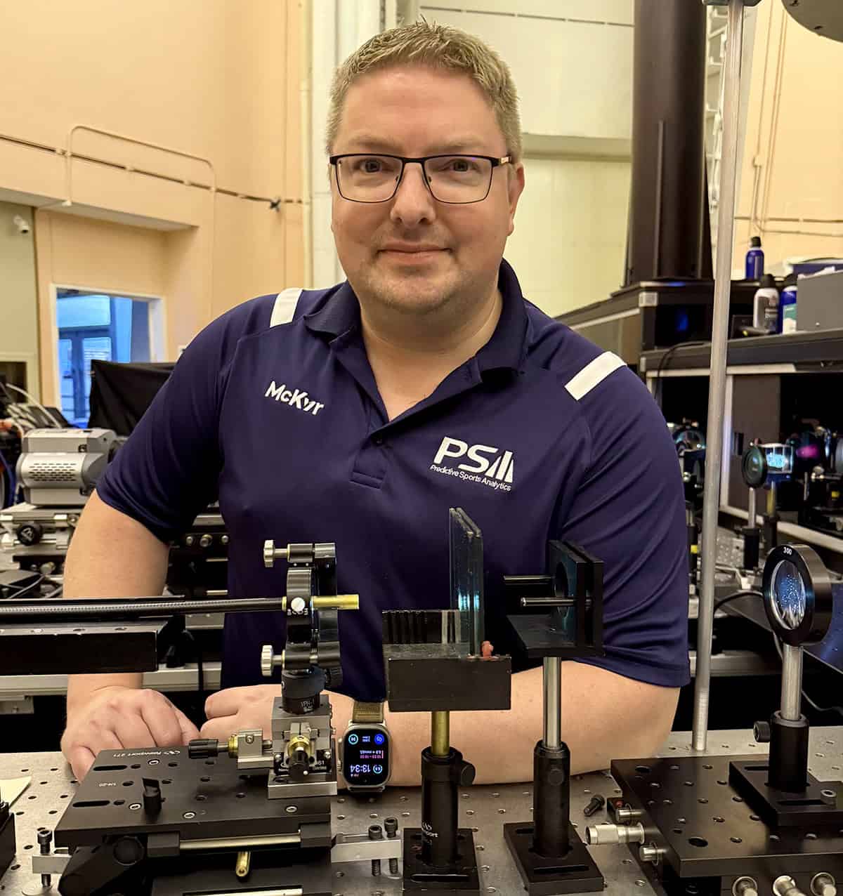
If David Jess were a professional footballer – and not a professional physicist – he’d probably be a creative midfielder: someone who links defence and attack to set up goal-scoring opportunities for his team mates. Based in the Astrophysics Research Centre at Queen’s University Belfast (QUB), Northern Ireland, Jess orchestrates his scientific activities in much the same way. Combining vision, awareness and decision-making, he heads a cross-disciplinary research team pursuing two very different and seemingly unconnected lines of enquiry.
Jess’s research within the QUB’s solar-physics groups centres on optical studies of the Sun’s lower atmosphere. That involves examining how the Sun’s energy travels through its near environment – in the form of both solar flares and waves. In addition, his group is developing instruments to support international research initiatives in astrophysics, including India’s upcoming National Large Solar Telescope.
But Jess is also a founding member of the Predictive Sports Analytics (PSA) research group within QUB and Ulster University’s AI Collaboration Centre – a £16m R&D facility supporting the adoption of AI and machine-learning technologies in local industry. PSA links researchers from a mix of disciplines – including physics, mathematics, statistics and computer science – with sports scientists in football, rugby, cycling and athletics. Its goal is to advance the fundamental science and application of predictive modelling in sports and health metrics.
Joined-up thinking
Astronomy and sports science might seem worlds apart, but they have lots in common, not least because both yield vast amounts of data. “We’re lucky,” says Jess. “Studying the closest star in the solar system means we are not photon-starved – there’s no shortage of light – and we are able to make observations of the Sun’s atmosphere at very high frame rates, which means we’re accustomed to managing and manipulating really big data sets.”
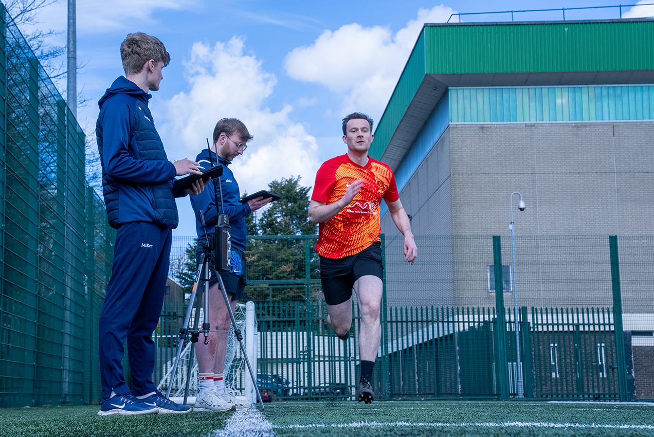
Similarly, big data also fuels the sports analytics industry. Many professional athletes wear performance-tracking sports vests with embedded GPS trackers that can generate tens of millions of data points over the course of, say, a 90-minute football match. The trackers capture information such as a player’s speed, their distance travelled, and the number of sprints and high-intensity runs.
“Trouble is,” says Jess, “you’re not really getting the ebb and flow of all that data by just summing it all up into the ‘one big number’.” Researchers in the PSA group are therefore trying to understand how athlete data evolves over time – often in real-time – to see if there’s some nuance or wrinkle that’s been missed in the “big-picture” metrics that emerge at the end of a game or training session.
It’s all in the game for PSA
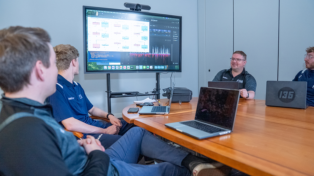
Set up in 2023, the Predictive Sports Analysis (PSA) research group in Belfast has developed collaborations with professional football teams, rugby squads and other sporting organizations across Northern Ireland and beyond. From elite-level to grassroots sports, real-world applications of PSA’s research aim to give athletes and coaches a competitive edge. Current projects include:
- Player/squad speed distribution analyses to monitor strength and conditioning improvements with time (also handy for identifying growth and performance trajectories in youth sport)
- Longitudinal examination of acceleration intensity as a proxy for explosive strength, which correlates with heart-rate variability (a useful aid to alert coaching staff to potential underlying cardiac conditions)
- 3D force vectorization to uncover physics-based thresholds linked to concussion and musculoskeletal injury in rugby
The group’s work might, for example, make it possible not only to measure how tired a player becomes after a 90-minute game but also to pinpoint the rates and causes of fatigue during the match. “Insights like this have the power to better inform coaching staff so they can create bespoke training regimes to target these specific areas,” adds Jess.
Work at PSA involves a mix of data mining, analysis, interpretation and visualization – teasing out granular insights from raw, unfiltered data streams by adapting and applying tried-and-tested statistical and mathematical methods from QUB’s astrophysics research. Take, for example, observational studies of solar flares – large eruptions of electromagnetic radiation from the Sun’s atmosphere lasting for a few minutes up to several hours.
“We might typically capture a solar-flare event at multiple wavelengths – optical, X-ray and UV, for example – to investigate the core physical processes from multiple vantage points,” says Jess. In other words, they can see how one wavelength component differs from another or how the discrete spectral components correlate and influence each other. “Statistically, that’s not so different from analysing the player data during a football match, with each player offering a unique vantage point in terms of the data points they generate,” he adds.
If that sounds like a stretch, Jess insists that PSA is not an indulgence or sideline. “We are experts in big data at PSA and, just as important, all of us have a passion for sports,” says Jess, who is a big fan of Chelsea FC. “What’s more, knowledge transfer between QUB’s astrophysics and sports analytics programmes works in both directions and delivers high-impact research dividends.”
The benefits of association
In-house synergies are all well and good, but the biggest operational challenge for PSA since it was set up in 2023 has been external. As a research group in QUB’s School of Mathematics and Physics, Jess and colleagues need to find ways to “get in the door” with prospective clients and clubs in the professional sports community. Bridging that gap isn’t straightforward for a physics lab that isn’t established in the sports-analytics business.
But clear communication as well as creative and accessible data visualization can help successful engagement. “Whenever we meet sports scientists at a professional club, the first thing we tell them is we’re not trying to do their job,” says Jess. “Rather, it’s about making their job easier to do and putting more analytical tools at their disposal.”
PSA’s skill lies in extracting “hidden signals” from big data sets to improve how athlete performance is monitored. Those insights can then be used by coaches, physiotherapists and medical staff to optimize training and recovery schedules as well as to improve the fitness, health and performance of individual athletes and teams.
Validation is everything in the sports analytics business, however, and the barriers to entry are high. That’s one reason why PSA’s R&D collaboration with STATSports could be a game-changer. Founded in 2007 in Newry, Northern Ireland, the company makes wearable devices that record and transmit athlete performance metrics hundreds of times each second.
STATSports is now a global leader in athlete monitoring and GPS performance analysis. Its technology is used by elite football clubs such as Manchester City, Liverpool, Arsenal and Juventus, as well as national football teams (including England, Argentina, USA and Australia) and leading teams in rugby and American football.
The tie-up lets PSA work with an industry “name”, while STATSports gets access to blue-sky research that could translate into technological innovation and commercial opportunities.
“PSA is an academic research team first and foremost, so we don’t want to just rest on our laurels,” explains Jess. “With so much data – whether astrophysics or sports analytics – we want to be at the cutting edge and deliver new advances that loop back to enhance the big data techniques we’re developing.”
Right now, PhD physicist Eamon McGleenan provides the direct line from PSA into STATSports, which is funding his postgraduate work. The joint research project, which also involves sports scientists from Saudi Pro League football club Al Qadsiah, uses detailed data about player sprints during a game. The aim is to use force, velocity and acceleration curves – as well as the power generated by a player’s legs – to evaluate the performance metrics that underpin athlete fatigue.
By reviewing these metrics during the course of a game, McGleenan and colleagues can model how an athlete’s performance drops off in real-time, indicating their level of fatigue. The hope is that the research will lead to in-game modelling systems to help coaches and medical staff at pitch-side to make data-driven decisions about player substitutions (rather than just taking a player off because they “look leggy”).
Six physicists who also succeeded at sport

Quantum physicist Niels Bohr was a keen footballer, who played in goal for Danish side Akademisk Boldklub in the early 1900s. He once let a goal in because he was more focused on solving a maths problem mid-game by scribbling calculations on the goal post. His mathematician brother Harald Bohr also played for the club and won silver at the 1908 London Olympics for the Danish national team.
Jonathan Edwards, who originally studied physics at Durham University, still holds the men’s world record for the triple-jump. Edwards broke the record twice on 7 August 1995 at the World Athletics Championships in Gothenburg, Sweden, first jumping 18.16m and then 18.29m barely 20 minutes later.
David Florence, who studied physics at the University of Nottingham, won silver in the single C1 canoe slalom at the Beijing Olympics in 2008. He also won silver in the doubles C2 slalom at the 2012 Olympics in London and in Rio de Janeiro four years later.
Louise Shanahan is a middle-distance runner who competed for Ireland in the women’s 800m race at the delayed 2020 Summer Olympics while still doing a PhD in physics on the properties of nanodiamonds at the University of Cambridge. She has recently set up a sports website called TrackAthletes.
US professional golfer Bryson DeChambeau is nicknamed “The Scientist” owing to his analytical, science-based approach to the sport – and the fact that he majored in physics at Southern Methodist University in Dallas, US. DeChambeau won the 2020 and 2024 US Open.
In 2023 Harvard University’s Jenny Hoffman, who studies the electronic properties of exotic materials, became the fastest woman to run across the US, completing the 5000 km journey in 47 days, 12 hours and 35 minutes. In doing so, she beat the previous record by more than a week.
Matin Durrani
The transfer market
Jess says that the PSA group has been inundated with applications from physics students since it was set up. That’s not surprising, argues Jess, given that a physics degree provides many transferable skills to suit PSA’s broad scientific remit. Those skills include being able to manage, mine and interpret large data sets; disseminate complex results and actionable insights to a non-specialist audience; and work with industry partners in the sports technology sector.
“We’re looking for multidisciplinarians at PSA,” says Jess, with a nod to his group’s ongoing PhD recruitment opportunities. “The ideal candidates will be keen to move beyond their existing knowledge base in physics and maths to develop skills in other specialist fields.” There have also been discussions with QUB’s research and enterprise department about the potential for a PSA spin-out venture – though Jess, for his part, remains focused on research.
“My priority is to ensure the sustainability of PSA,” he concludes. “That means more grant funding – whether from the research councils or industry partners – while training up the next generation of early-career researchers. Longer term, though, I do think that PSA has the potential to be a ‘disruptor’ in the sports-analytics industry.”