Spooky physics: from glowing green bats to vibrating spider webs

It’s Halloween today and so what better time than to bring you a couple of spooky stories from the world of physics.

First up is researchers at the University of Georgia in the US who have confirmed that six different species of bats found in North America emit a ghoulish green light when exposed to ultraviolet light.

The researchers examined 60 specimens from the Georgia Museum of Natural History and exposed the bats to UV light.

They found that the wings and hind limbs of six species – big brown bats, eastern red bats, Seminole bats, southeastern myotis, grey bats and the Brazilian free-tailed bat – gave off photoluminescence with the resulting glow being a shade of green.

While previous research found that some mammals, like pocket gophers, also emit a glow under ultraviolet light, this was the first discovery of such a phenomenon for bats located in North America.

The colour and location of the glow on the winged mammals suggest it is not down to genetics or camouflage and as it is the same between sexes it is probably not used to attract mates.

“It may not seem like this has a whole lot of consequence, but we’re trying to understand why these animals glow,” notes wildlife biologist Steven Castleberry from the University of Georgia.

Given that many bats can see the wavelengths emitted, one option is that the glow may be an inherited trait used for communication.

“The data suggests that all these species of bats got it from a common ancestor. They didn’t come about this independently,” adds Castleberry. “It may be an artifact now, since maybe glowing served a function somewhere in the evolutionary past, and it doesn’t anymore.”

Thread lightly

In other frightful news, spider webs are a classic Halloween decoration and while the real things are marvels of bioengineering, there is still more to understand about these sticky structures.

Many spider species build spiral wheel-shaped webs – orb webs – to capture prey, and some incorporate so-called “stabilimenta” into their web structure. These “extra touches” look like zig-zagging threads that span the gap between two adjacent “spokes,” or threads arranged in a circular “platform” around the web’s centre.

The purpose of stabilimenta is unknown and proposed functions include as a deterrence for predatory wasps or birds.

Yet Gabriele Greco of the Swedish University of Agricultural Sciences and colleagues suggest such structures might instead influence the propagation of web vibrations triggered by the impact of captured prey.

Greco and colleagues observed different stabilimentum geometries that were constructed by wasp spiders, Argiope bruennichi. The researchers then performed numerical simulations to explore how stabilimenta affect prey impact vibrations.

For waves generated at angles perpendicular to the threads spiralling out from the web centre, stabilimenta caused negligible delays in wave propagation.

However, for waves generated in the same direction as the spiral threads, vibrations in webs with stabilimenta propagated to a greater number of potential detection points across the web – where a spider might sense them – than in webs without stabilimenta.

This suggests that stabilimenta may boost a spider’s ability to pinpoint the location of unsuspecting prey caught in its web.

Spooky.

Lowering exam stakes could cut the gender grade gap in physics, finds study

Female university students do much better in introductory physics exams if they have the option of retaking the tests. That’s according to a new analysis of almost two decades of US exam results for more than 26,000 students. The study’s authors say it shows that female students benefit from lower-stakes assessments – and that the persistent “gender grade gap” in physics exam results does not reflect a gender difference in physics knowledge or ability.

The study has been carried out by David Webb from the University of California, Davis, and Cassandra Paul from San Jose State University. It builds on previous work they did in 2023, which showed that the gender gap disappears in introductory physics classes that offer the chance for all students to retake the exams. That study did not, however, explore why the offer of a retake has such an impact.

In the new study, the duo analysed exam results from 1997 to 2015 for a series of introductory physics classes at a public university in the US. The dataset included 26,783 students, mostly in biosciences, of whom about 60% were female. Some of the classes let students retake exams while others did not, thereby letting the researchers explore why retakes close the gender gap.

When Webb and Paul examined the data for classes that offered retakes, they found that in first-attempt exams female students slightly outperformed their male counterparts. But male students performed better than female students in retakes.

This, the researchers argue, discounts the notion that retakes close the gender gap by allowing female students to improve their grades. Instead, they suggest that the benefit of retakes is that they lower the stakes of the first exam.

The team then compared the classes that offered retakes with those that did not, which they called high-stakes courses. They found that the gender gap in exam results was much larger in the high-stakes classes than the lower-stakes classes that allowed retakes.

“This suggests that high-stakes exams give a benefit to men, on average, [and] lowering the stakes of each exam can remove that bias,” Webb told Physics World. He thinks that as well as allowing students to retake exams, physics might benefit from not having comprehensive high-stakes final exams but instead “use final exam time to let students retake earlier exams”.

Quantum steampunk: we explore the art and science

Earlier this year I met the Massachusetts-based steampunk artist Bruce Rosenbaum at the Global Physics Summit of the American Physical Society. He was exhibiting a beautiful sculpture of a “quantum engine” that was created in collaboration with physicists including NIST’s Nicole Yunger Halpern – who pioneered the scientific field of quantum steampunk.

I was so taken by the art and science of quantum steampunk that I promised Rosenbaum that I would chat with him and Yunger Halpern on the podcast – and here is that conversation. We begin by exploring the art of steampunk and how it is influenced by the technology of the 19th century. Then, we look at the physics of quantum steampunk, a field that weds modern concepts of quantum information with thermodynamics – which itself is a scientific triumph of the 19th century.


This podcast is supported by Atlas Technologies, specialists in custom aluminium and titanium vacuum chambers as well as bonded bimetal flanges and fittings used everywhere from physics labs to semiconductor fabs.

Quantum fluids mix like oil and water

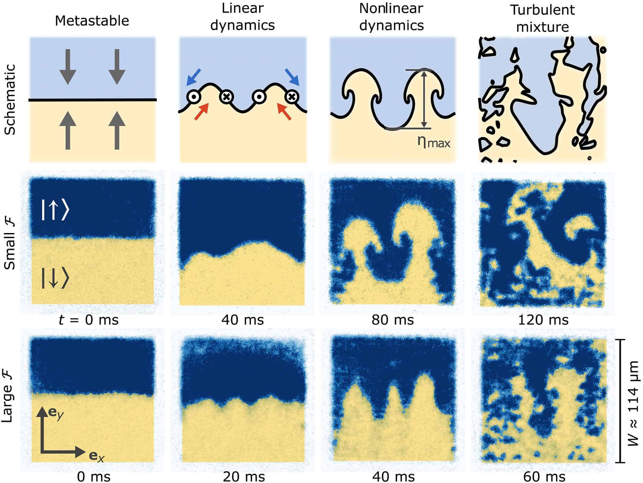
A grid of diagrams and data showing how the system evolves from a metastable state in which two components, coloured blue and yellow, are stacked on top of each other and separated like oil and water, into a turbulent mixture where blobs of yellow and blue are all over the place. At the interim stages, a small applied disturbing force creates mushroom-like bulges of the yellow fluid into the blue fluid, while a larger force produces finger-like pillars.

Researchers in the US have replicated a well-known fluid-dynamics process called the Rayleigh–Taylor instability on a quantum scale for the first time. The work opens the hydrodynamics of quantum gases to further exploration and could even create a new platform for understanding gravitational dynamics in the early universe.

If you’ve ever tried mixing oil with water, you’ll understand how the Rayleigh–Taylor instability (RTI) can develop. Due to their different molecular structures and the nature of the forces between their molecules, the two fluids do not mix well. After some time, they separate, forming a clear interface between oil and water.

Scientists have studied the dynamics of this interface upon perturbations – disturbances of the system – for nearly 150 years, with major work being done by the British physicists Lord Rayleigh in 1883 and Geoffrey Taylor in 1950. Under specific conditions related to the buoyant force of the fluid and the perturbative force causing the disturbance, they showed that this interface becomes unstable. Rather than simply oscillating, the system deviates from its initial state, leading to the formation of interesting geometric patterns such as mushroom clouds and filaments of gas in the Crab Nebula.

An interface of spins

To show that such dynamics occur not only in macroscopic structures, but also at a quantum scale, scientists at the University of Maryland and the Joint Quantum Institute (JQI) created a two-state quantum system using a Bose–Einstein condensate (BEC) of sodium (23Na) atoms. In this state of matter, the temperature is so low, the sodium atoms behave as a single coherent system, giving researchers precise control of their parameters.

The JQI team confine this BEC in a two-dimensional optical potential that essentially produces a 100 µm × 100 µm sheet of atoms in the horizontal plane. The scientists then apply a microwave pulse that excites half of the atoms from the spin-down to the spin-up state. By adding a small magnetic field gradient along one of the horizontal axes, they induce a force (the Stern–Gerlach force) that acts on the two spin components in opposite directions due to the differing signs of their magnetic moments. This creates a clear interface between the spin-up and the spin-down atoms.

Mushrooms and ripplons

To initiate the RTI, the scientists need to perturb this two-component BEC by reversing the magnetic field gradient, which consequently reverses the direction of the induced force. According to Ian Spielman, who led the work alongside co-principal investigator Gretchen Campbell, this wasn’t as easy as it sounds. “The most difficult part was preparing the initial state (horizontal interface) with high quality, and then reliably inverting the gradient rapidly and accurately,” Spielman says.

The researchers then investigated how the magnitude of this force difference, acting on the two sides of the interface, affected the dynamics of the two-component BEC. For a small differential force, they initially observed a sinusoidal modulation of the interface. After some time, the interface enters a nonlinear dynamics regime where the RTI manifests through the formation of mushroom clouds. Finally, it becomes a turbulent mixture. The larger the differential force, the more rapidly the system evolves.

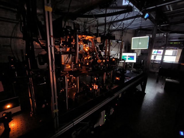
Photo of a darkened optics laboratory with screens and a vacuum system. The scene is bathed in orange light from the lasers used

While RTI dynamics like these were expected to occur in quantum fluids, Spielman points out that proving it required a BEC with the right internal interactions. The BEC of sodium atoms in their experimental setup is one such system.

In general, Spielman says that cold atoms are a great tool for studying RTI because the numerical techniques used to describe them do not suffer from the same flaws as the Navier–Stokes equation used to model classical fluid dynamics. However, he notes that the transition to turbulence is “a tough problem that resides at the boundary between two conceptually different ways of thinking”, pushing the capabilities of both analytical and numerical techniques.

The scientists were also able to excite waves known as ripplon modes that travel along the interface of the two-component BEC. These are equivalent to the classical capillary waves –“ripples” when a droplet impacts a water surface. Yanda Geng, a JQI PhD student working on this project, explains that every unstable RTI mode has a stable ripplon as a sibling. The difference is that ripplon modes only appear when a small sinusoidal modulation is added to the differential force. “Studying ripplon modes builds understanding of the underlying [RTI] mechanism,” Geng says.

The flow of the spins

In a further experiment, the team studied a phenomenon that occurs as the RTI progresses and the spin components of the BEC flow in opposite directions along part of their shared interface. This is known as an interfacial counterflow. By transferring half the atoms into the other spin state after initializing the RTI process, the scientists were able to generate a chain of quantum mechanical whirlpools – a vortex chain – along the interface in regions where interfacial counterflow occurred.

Spielman, Campbell and their team are now working to create a cleaner interface in their two-component BEC, which would allow a wider range of experiments. “We are considering the thermal properties of this interface as a 1D quantum ‘string’,” says Spielman, adding that the height of such an interface is, in effect, an ultra-sensitive thermometer. Spielman also notes that interfacial waves in higher dimensions (such as a 2D surface) could be used for simulations of gravitational physics.

The research is described in Science Advances.

Large-area triple-junction perovskite solar cell achieves record efficiency

Improving the efficiency of solar cells will likely be one of the key approaches to achieving net zero emissions in many parts of the world. Many types of solar cells will be required, with some of the better performances and efficiencies expected to come from multi-junction solar cells. Multi-junction solar cells comprise a vertical stack of semiconductor materials with distinct bandgaps, with each layer converting a different part of the solar spectrum to maximize conversion of the Sun’s energy to electricity.

When there are no constraints on the choice of materials, triple-junction solar cells can outperform double-junction and single-junction solar cells, with a power conversion efficiency (PCE) of up to 51% theoretically possible. But material constraints – due to fabrication complexity, cost or other technical challenges – mean that many such devices still perform far from the theoretical limits.

Perovskites are one of the most promising materials in the solar cell world today, but fabricating practical triple-junction solar cells beyond 1 cm2 in area has remained a challenge. A research team from Australia, China, Germany and Slovenia set out to change this, recently publishing a paper in Nature Nanotechnology describing the largest and most efficient triple-junction perovskite–perovskite–silicon tandem solar cell to date.

When asked why this device architecture was chosen, Anita Ho-Baillie, one of the lead authors from The University of Sydney, states: “I am interested in triple-junction cells because of the larger headroom for efficiency gains”.

Addressing surface defects in perovskite solar cells

Solar cells formed from metal halide perovskites have potential to be commercially viable, due to their cost-effectiveness, efficiency, ease of fabrication and their ability to be paired with silicon in multi-junction devices. The ease of fabrication means that the junctions can be directly fabricated on top of each other through monolithic integration – which leads to only two terminal connections, instead of four or six. However, these junctions can still contain surface defects.

To enhance the performance and resilience of their triple-junction cell (top and middle perovskite junctions on a bottom silicon cell), the researchers optimized the chemistry of the perovskite material and the cell design. They addressed surface defects in the top perovskite junction by replacing traditional lithium fluoride materials with piperazine-1,4-diium chloride (PDCl). They also replaced methylammonium – which is commonly used in perovskite cells – with rubidium. “The rubidium incorporation in the bulk and the PDCl surface treatment improved the light stability of the cell,” explains Ho-Baillie.

To connect the two perovskite junctions, the team used gold nanoparticles on tin oxide. Because the gold was in a nanoparticle form, the junctions could be engineered to maximize the flow of electric charge and light absorption by the solar cell.

“Another interesting aspect of the study is the visualization of the gold nanoparticles [using transmission electron microscopy] and the critical point when they become a semi-continuous film, which is detrimental to the multi-junction cell performance due to its parasitic absorption,” says Ho-Baillie. “The optimization for achieving minimal particle coverage while achieving sufficient ohmic contact for vertical carrier flow are useful insights”.

Record performance for a large-scale perovskite triple-junction cell

Using these design strategies, Ho-Baillie and colleagues developed a 16 cm2 triple-junction cell that achieved an independently certified steady-state PCE of 23.3% – the highest reported for a large-area device. While triple-junction perovskite solar cells have exhibited higher PCEs – with all-perovskite triple-junction cells reaching 28.7% and perovskite–perovskite–silicon devices reaching 27.1% – these were all achieved on a 1 cm2 cell, not a large-area cell.

In this study, the researchers also developed a 1 cm2 cell that was close to the best, with a PCE of 27.06%, but it is the large-area cell that’s the record breaker. The 1 cm2 cell also passed the International Electrotechnical Commission’s (IEC) 61215 thermal cycling test, which exposes the cell to 200 cycles under extreme temperature swings, ranging from –40 to 85°C. During this test, the 1 cm2 cell retained 95% of its initial efficiency after 407 h of continuous operation.

The combination of the successful thermal cycling test combined with the high efficiencies on a larger cell shows that there could be potential for this triple-junction architecture in real-world settings in the near future, even though they are still far away from their theoretical limits.

Tim Berners-Lee: why the inventor of the Web is ‘optimistic, idealistic and perhaps a little naïve’

It’s rare to come across someone who’s been responsible for enabling a seismic shift in society that has affected almost everyone and everything. Tim Berners-Lee, who invented the World Wide Web, is one such person. His new memoir This is for Everyone unfolds the history and development of the Web and, in places, of the man himself.

Berners-Lee was born in London in 1955 to parents, originally from Birmingham, who met while working on the Ferranti Mark 1 computer and knew Alan Turing. Theirs was a creative, intellectual and slightly chaotic household. His mother could maintain a motorbike with fence wire and pliers, and was a crusader for equal rights in the workplace. His father – brilliant and absent minded – taught Berners-Lee about computers and queuing theory. A childhood of camping and model trains, it was, in Berners-Lee’s view, idyllic.

Berners-Lee had the good fortune to be supported by a series of teachers and managers who recognized his potential and unique way of working. He studied physics at the University of Oxford (his tutor “going with the flow” of Berners-Lee’s unconventional notation and ability to approach problems from oblique angles) and built his own computer. After graduating, he married and, following a couple of jobs, took a six-month placement at the CERN particle-physics lab in Geneva in 1985.

This placement set “a seed that sprouted into a tool that shook up the world”. Berners-Lee saw how difficult it was to share information stored in different languages in incompatible computer systems and how, in contrast, information flowed easily when researchers met over coffee, connected semi-randomly and talked. While at CERN, he therefore wrote a rough prototype for a program to link information in a type of web rather than a structured hierarchy.

Back at CERN, Tim Berners-Lee developed his vision of a “universal portal” to information

The placement ended and the program was ignored, but four years later Berners-Lee was back at CERN. Now divorced and soon to remarry, he developed his vision of a “universal portal” to information. It proved to be the perfect time. All the tools necessary to achieve the Web – the Internet, address labelling of computers, network cables, data protocols, the hypertext language that allowed cross-referencing of text and links on the same computer – had already been developed by others.

Berners-Lee saw the need for a user-friendly interface, using hypertext that could link to information on other computers across the world. His excitement was “uncontainable”, and according to his line manager “few of us if any could understand what he was talking about”. But Berners-Lee’s managers supported him and freed his time away from his actual job to become the world’s first web developer.

Having a vision was one thing, but getting others to share it was another. People at CERN only really started to use the Web properly once the lab’s internal phone book was made available on it. As a student at the time, I can confirm that it was much, much easier to use the Web than log on to CERN’s clunky IBM mainframe, where phone numbers had previously been stored.

Wider adoption relied on a set of volunteer developers, working with open-source software, to make browsers and platforms that were attractive and easy to use. CERN agreed to donate the intellectual property for web software to the public domain, which helped. But the path to today’s Web was not smooth: standards risked diverging and companies wanted to build applications that hindered information sharing.

Feeling that “the Web was outgrowing my institution” and “would be a distraction” to a lab whose core mission was physics, Berners-Lee moved to the Massachusetts Institute of Technology in 1994. There he founded the World Wide Web Consortium (W3C) to ensure consistent, accessible standards were followed by everyone as the Web developed into a global enterprise. The progression sounds straightforward although earlier accounts, such as James Gillies and Robert Caillau’s 2000 book How the Web Was Born, imply some rivalry between institutions that is glossed over here.

Initially inclined to advise people to share good things and not search for bad things, Berners-Lee had reckoned without the insidious power of “manipulative and coercive” algorithms on social networks

The rest is history, but not quite the history that Berners-Lee had in mind. By 1995 big business had discovered the possibilities of the Web to maximize influence and profit. Initially inclined to advise people to share good things and not search for bad things, Berners-Lee had reckoned without the insidious power of “manipulative and coercive” algorithms on social networks. Collaborative sites like Wikipedia are closer to his vision of an ideal Web; an emergent good arising from individual empowerment. The flip side of human nature seems to come as a surprise.

The rest of the book brings us up to date with Berners-Lee’s concerns (data, privacy, misuse of AI, toxic online culture), his hopes (the good use of AI), a third marriage and his move into a data-handling business. There are some big awards and an impressive amount of name dropping; he is excited by Order of Merit lunches with the Queen and by sitting next to Paul McCartney’s family at the opening ceremony to the London Olympics in 2012. A flick through the index reveals names ranging from Al Gore and Bono to Lucien Freud. These are not your average computing technology circles.

There are brief character studies to illustrate some of the main players, but don’t expect much insight into their lives. This goes for Berners-Lee too, who doesn’t step back to particularly reflect on those around him, or indeed his own motives beyond that vision of a Web for all enabling the best of humankind. He is firmly future focused.

Still, there is no-one more qualified to describe what the Web was intended for, its core philosophy, and what caused it to develop to where it is today. You’ll enjoy the book whether you want an insight into the inner workings that make your web browsing possible, relive old and forgotten browser names, or see how big tech wants to monetize and monopolize your online time. It is an easy read from an important voice.

The book ends with a passionate statement for what the future could be, with businesses and individuals working together to switch the Web from “the attention economy to the intention economy”. It’s a future where users are no longer distracted by social media and manipulated by attention-grabbing algorithms; instead, computers and services do what users want them to do, with the information that users want them to have.

Berners-Lee is still optimistic, still an incurable idealist, still driven by vision. And perhaps still a little naïve too in believing that everyone’s values will align this time.

  • 2025 Macmillan 400pp £25.00/$30.00hb

New protocol makes an elusive superconducting signature measurable

Conversion of a hard-to-detect signal into a pattern that reveals d-wave pairing

Understanding the mechanism of high-temperature superconductivity could unlock powerful technologies, from efficient energy transmission to medical imaging, supercomputing and more. Researchers at Harvard University and the Massachusetts Institute of Technology have designed a new protocol to study a candidate model for high-temperature superconductivity (HTS), described in Physical Review Letters.

The model, known as the Fermi-Hubbard model, is believed to capture the essential physics of cuprate high-temperature superconductors, materials composed of copper and oxygen. The model describes fermions, such as electrons, moving on a lattice. The fermions experience two competing effects: tunnelling and on-site interaction. Imagine students in a classroom: they may expend energy to switch seats (tunnelling), avoid a crowded desk (repulsive on-site interaction) or share desks with friends (attractive on-site interaction). Such behaviour mirrors that of electrons moving between lattice sites.

Daniel Mark, first author of the study, notes that: “After nearly four decades of research, there are many detailed numerical studies and theoretical models on how superconductivity can emerge from the Fermi-Hubbard model, but there is no clear consensus [on exactly how it emerges].”

A precursor to understanding the underlying mechanism is testing whether the Fermi-Hubbard model gives rise to an important signature of cuprate HTS: d-wave pairing. This is a special type of electron pairing where the strength and sign of the pairing depend on the direction of electron motion. It contrasts with conventional low-temperature superconductors that exhibit s-wave pairing, in which the pairing strength is uniform in all directions.

Although physicists have developed robust methods for simulating the Fermi-Hubbard model with ultracold atoms, measuring d-wave pairing has been notoriously difficult. The new protocol aims to change that.

A change of perspective

A key ingredient in the protocol is the team’s use of “repulsive-to-attractive mapping”. The physics of HTS is often described by the repulsive Fermi-Hubbard model, in which electrons pay an energetic penalty for occupying the same lattice site, like disagreeing students sharing a desk. In this model, detecting d-wave pairing requires fermions to maintain a fragile quantum state as they move over large distances, which necessitates carefully fine-tuned experimental parameters.

To make the measurement more robust to experimental imperfection, the authors use a clever mathematical trick: they map from the repulsive model to the attractive one. In the attractive model, electrons receive an energetic benefit from being close together, like two friends in a classroom. The mapping is achieved by a particle–hole transformation, wherein spin-down electrons are reinterpreted as holes and vice versa. After mapping, the d-wave pairing signal becomes an observable that conserves local fermion number, thereby circumventing the challenge of long-range motion.

Pulse sequence

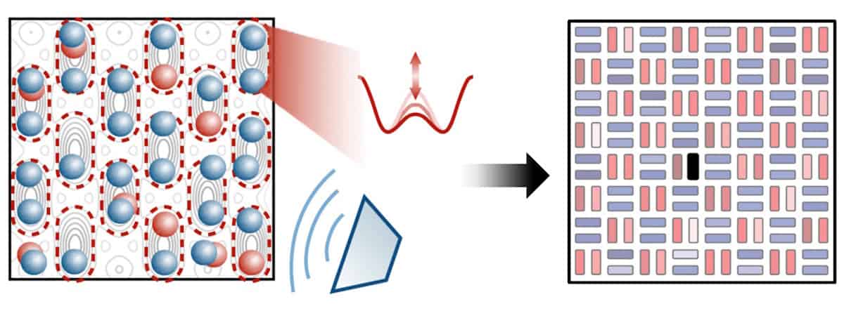
In its initial form, the d-wave pairing signal is difficult to measure. Drawing inspiration from digital quantum gates, the researchers divide their complex system into subsystems composed of pairs of lattice sites or dimers. Then, they apply a pulse sequence to make the observable measurable by simply counting fermions – a standard technique in the lab.

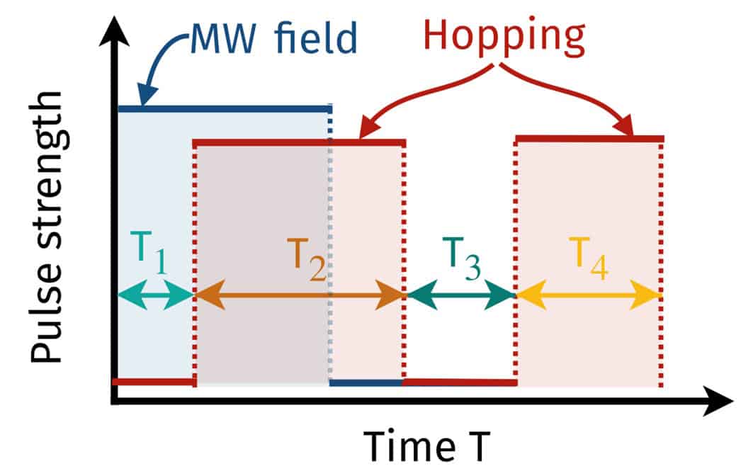
The pulse sequence begins with a global microwave pulse to manipulate the spin of the fermions, followed by a series of “hopping” and “idling” steps. The hopping step involves lowering the barrier between lattice sites, thereby increasing tunnelling. The idling step involves raising the barrier, allowing the system to evolve without tunnelling. Every step is carefully timed to reveal the d-wave pairing information at the end of the sequence.

The researchers report that their protocol is sample-efficient, experimentally viable, and generalizable to other observables that conserve local fermion number and act on dimers.

This work adds to a growing field that combines components of analogue quantum systems with digital gates to deeply study complex quantum phenomena. “All the experimental ingredients in our protocol have been demonstrated in existing experiments, and we are in discussion with several groups on possible use cases,” Mark tells Physics World.

Interface engineered ferromagnetism

Exchange-coupled interfaces offer a powerful route to stabilising and enhancing ferromagnetic properties in two-dimensional materials, such as transition metal chalcogenides. These materials exhibit strong correlations among charge, spin, orbital, and lattice degrees of freedom, making them an exciting area for emergent quantum phenomena.

Cr₂Te₃’s crystal structure naturally forms layers that behave like two-dimensional sheets of magnetic material. Each layer has magnetic ordering (ferromagnetism), but the layers are not tightly bonded in the third dimension and are considered “quasi-2D.” These layers are useful for interface engineering. Using a vacuum-based technique for atomically precise thin-film growth, known as molecular beam epitaxy, the researchers demonstrate wafer-scale synthesis of Cr₂Te₃ down to monolayer thickness on insulating substrates. Remarkably, robust ferromagnetism persists even at the monolayer limit, a critical milestone for 2D magnetism.

When Cr₂Te₃ is proximitized (an effect that occurs when one material is placed in close physical contact with another so that its properties are influenced by the neighbouring material) to a topological insulator, specifically (Bi,Sb)₂Te₃, the Curie temperature, the threshold between ferromagnetic and paramagnetic phases, increases from ~100 K to ~120 K. This enhancement is experimentally confirmed via polarized neutron reflectometry, which reveals a substantial boost in magnetization at the interface.

Theoretical modelling attributes this magnetic enhancement to the Bloembergen–Rowland interaction which is a long-range exchange mechanism mediated by virtual intraband transitions. Crucially, this interaction is facilitated by the topological insulator’s topologically protected surface states, which are spin-polarized and robust against disorder. These states enable long-distance magnetic coupling across the interface, suggesting a universal mechanism for Curie temperature enhancement in topological insulator-coupled magnetic heterostructures.

This work not only demonstrates a method for stabilizing 2D ferromagnetism but also opens the door to topological electronics, where magnetism and topology are co-engineered at the interface. Such systems could enable novel quantum hybrid devices, including spintronic components, topological transistors, and platforms for realizing exotic quasiparticles like Majorana fermions.

Read the full article

Enhanced ferromagnetism in monolayer Cr2Te3 via topological insulator coupling

Yunbo Ou et al 2025 Rep. Prog. Phys. 88 060501

Do you want to learn more about this topic?

Interacting topological insulators: a review by Stephan Rachel (2018)

Probing the fundamental nature of the Higgs Boson

First proposed in 1964, the Higgs boson plays a key role in explaining why many elementary particles of the Standard Model have a rest mass. Many decades later the Higgs boson was observed in 2012 by the ATLAS and CMS collaborations at the Large Hadron Collider (LHC), confirming the decades old prediction.  

This discovery made headline news at the time and, since then, the two collaborations have been performing a series of measurements to establish the fundamental nature of the Higgs boson field and of the quantum vacuum. Researchers certainly haven’t stopped working on the Higgs though. In subsequent years, a series of measurements have been performed to establish the fundamental nature of the new particle. 

One key measurement comes from studying a process known as off-shell Higgs boson production. This is the creation of Higgs bosons with a mass significantly higher than their typical on-shell mass of 125 GeV.  This phenomenon occurs due to quantum mechanics, which allows particles to temporarily fluctuate in mass.

This kind of production is harder to detect but can reveal deeper insights into the Higgs boson’s properties, especially its total width, which relates to how long it exists before decaying. This in turn, allows us to test key predictions made by the Standard Model of particle physics.

Previous observations of this process had been severely limited in their sensitivity. In order to improve on this, the ATLAS collaboration had to introduce a completely new way of interpreting their data (read here for more details).

They were able to provide evidence for off-shell Higgs boson production with a significance of 2.5𝜎 (corresponding to a 99.38% likelihood), using events with four electrons or muons, compared to a significance of 0.8𝜎 using traditional methods in the same channel.

The results mark an important step forward in understanding the Higgs boson as well as other high-energy particle physics phenomena.

Fabrication and device performance of Ni0/Ga2O3 heterojunction power rectifiers

Want to learn more about this webinar?

ecs webinar image

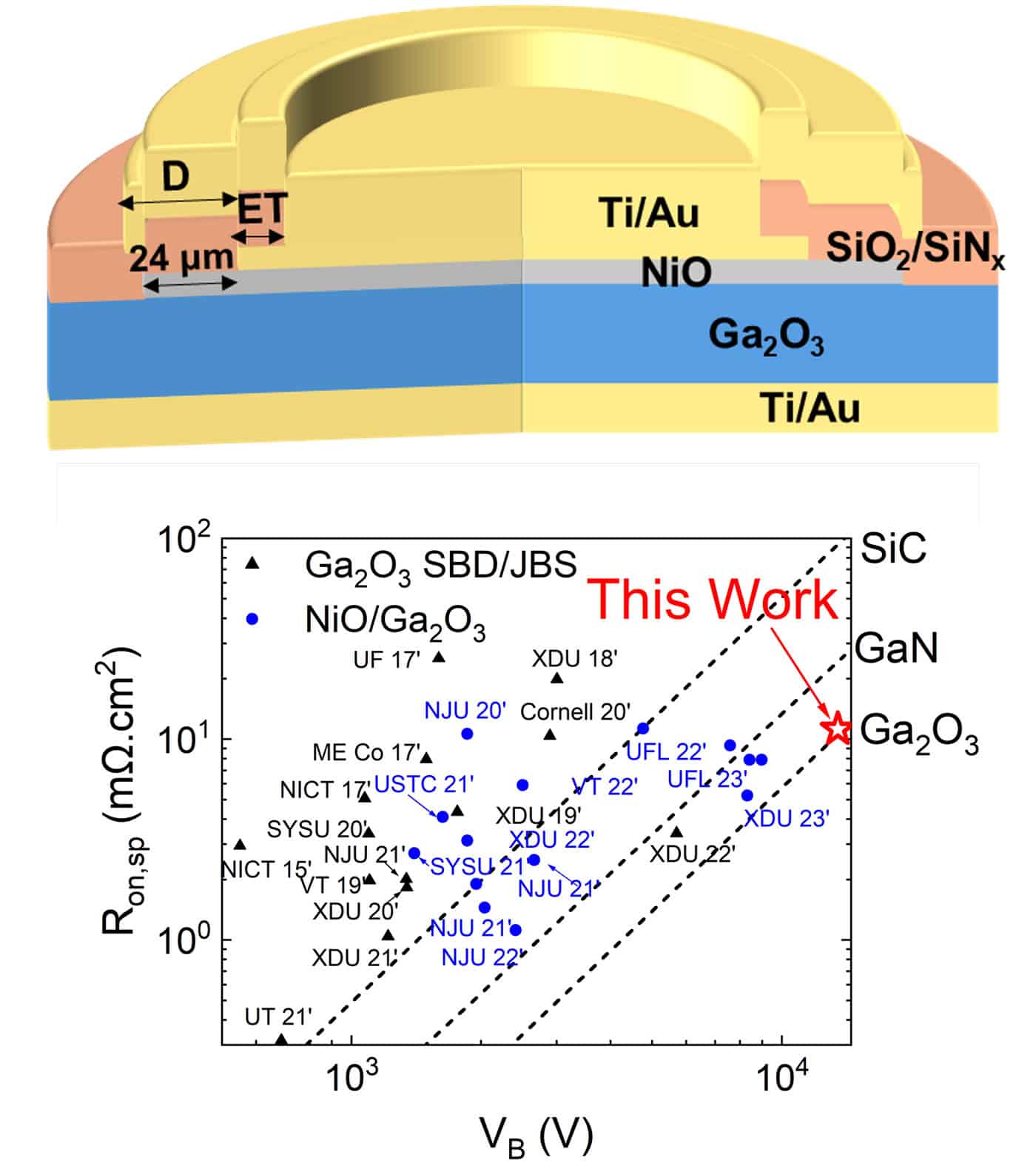
This talk shows how integrating p-type NiO to form NiO/GaO heterojunction rectifiers overcomes that barrier, enabling record-class breakdown and Ampere-class operation. It will cover device structure/process optimization, thermal stability to high temperatures, and radiation response – with direct ties to today’s priorities: EV fast charging, AI data‑center power systems, and aerospace/space‑qualified power electronics.

An interactive Q&A session follows the presentation.

Want to learn more about this webinar?


Jian-Sian Li received the PhD in chemical engineering from the University of Florida in 2024, where his research focused on NiO/β-GaO heterojunction power rectifiers, includes device design, process optimization, fast switching, high-temperature stability, and radiation tolerance (γ, neutron, proton). His work includes extensive electrical characterization and microscopy/TCAD analysis supporting device physics and reliability in harsh environments. Previously, he completed his BS and MS at National Taiwan University (2015, 2018), with research spanning phoretic/electrokinetic colloids, polymers for OFETs/PSCs, and solid-state polymer electrolytes for Li-ion batteries. He has since transitioned to industry at Micron Technology.

Copyright © 2026 by IOP Publishing Ltd and individual contributors