In the small country town of Bourne, Lincolnshire, just a minute’s walk from the high street, a steady stream of people are arriving at and leaving an attractive redbrick building that was originally a malthouse. It’s shift change at Warners Printers, which has printed every issue of Physics World for the last 30 years. I made the journey from Bristol last week to find out more about our longest-serving supplier, quiz them about their (excellent) environmental standards and – this is the fun bit – see the July issue of Physics World being printed before it’s posted out to members of the Institute of Physics later this week.
I was met by our account manager Adam Lees and introduced to the managing director Philip Warner, as well as his son Michael Warner who is the marketing manager. Adam and Michael showed me all seven of Warners’ printing presses – four web presses and three sheetfed (Physics World uses both kinds) – and gave me a refresher course on the whole offset printing process, from pre-press checks to final binding and packaging. It used to be standard practice for production managers like me to go to the printer on press day, but this was my first experience of seeing something on the press that I had produced myself and I was pretty excited.
The first stage is imposition. Apart from the cover, Physics World is printed in 16-page sections. A clever piece of software calculates which page goes where so that when the 16 pages are folded and stacked with all the other sections, the final result has all the pages in the correct order and the right way up. Warners always does a manual check of this stage. (In a previous life working in book publishing, one of my first tasks was checking that all the pages were in order – you’d be surprised how often this can go wrong.)
Sneak preview: the magenta plate of one of the sections of the July issue of Physics World. (Courtesy: Kate Gardner)
These impositions are sent to the plate-making room, where eight plates are made for each section: cyan, magenta, yellow and black; top and bottom. The plates are aluminium – Warners’ second biggest raw material, chosen because it’s lightweight, flexible and 100% recyclable. The plates have a thin coating of light-sensitive material. Exposure to light and chemicals means that the areas that need to be inked are made oleophilic and hydrophobic, while the areas that are not to be inked are made oleophobic and hydrophilic.
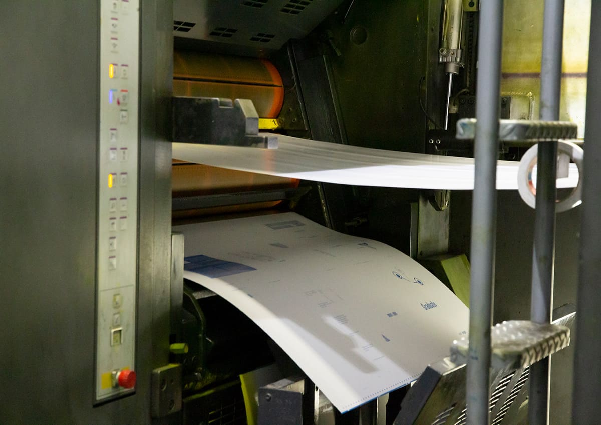
The plates are now loaded onto the press and wrapped around cylinders. The oil-based ink is attracted to the plate in all the right places and then transferred to a long reel of paper. On a web press, both sides of the paper are printed at the same time, in a sheet-to-sheet process that is extremely fast. A sheetfed press does the four colours on one side then flips the paper over to do the other side. This sheet-to-metal process is slower but slightly sharper – as well as being able to accommodate thicker paper – so it is mostly used for covers (including ours). At the end of the line, the printed sheets come out flat, with a tiny quantity of starch puffed in-between each to prevent them from sticking together.
Mechanically loading the first set of plates onto the web press. (Courtesy: Kate Gardner)
What I hadn’t realized before my visit is that the web presses, in contrast, dry and fold the sheets. After printing, the paper runs through a hot oven then onto cold rollers, all carefully calibrated for maximum drying with zero paper distortion. Puffs of air and vacuum are then used to fold the sheet. Blades and glue are applied so that the conveyor belt at the end of line carries running sheets already prepared for binding.
The web presses use puffs of air to fold each 16-page section so that the output is running sheets that are ready for binding. (Courtesy: Kate Gardner)
The web presses are newer technology, and as well as being fast, they also calibrate the inks more quickly each time they start up, which reduces paper wastage (as well as ink and electricity use). This is a big consideration for Warners, paper being by far its most used raw material. The biggest presses get through around 40 km of paper per hour. Each issue of Physics World uses approximately 4 tonnes of paper. All the waste paper is of course recycled (in fact, Warners reuses or recycles 99.98% of all its waste materials – the 0.02% being from spill kits or cleaning supplies) but work is ongoing to reduce waste in the first place. The paper is FSC or PEFC certified wherever possible.
Each issue of Physics World uses approximately 4 tonnes of paper. (Courtesy: Kate Gardner)
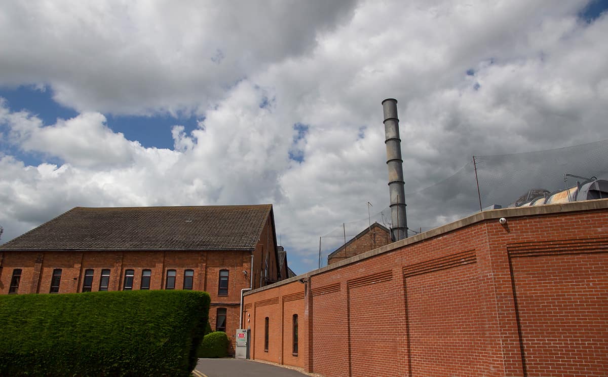
I was curious about the big chimneys in each of the printing halls. These are regenerative thermal oxidizers (RTOs), which break down any volatile organic compounds created by the presses. They use the calorific value of the gases they burn off to sustain themselves. Warners only uses electricity from renewable sources, which includes its own array of solar panels, and has been making great strides in reducing gas and electricity consumption.
The old building at Warners (left) was formerly a malthouse. On the right you can see one of the three chimneys that act as regenerative thermal oxidizers. (Courtesy: Kate Gardner)
We don’t use Warners for our distribution to members, but I was still curious to talk about packaging alternatives to plastic, as it’s something we’ve been looking into for the past year. It’s a more complex issue than it appears at first glance. You’ll be hearing more about that soon.
It was a great trip, and the sun came out in time for me to enjoy a stroll around the large Wellhead Gardens park next door to Warners before I headed home. It’s easy to see how this printing company has flourished where others have folded, and why we have stuck with the partnership for so long.
Is any scientific quest today more exciting than the search for life beyond Earth?
Here in Bellevue, Washington the answer is an emphatic “no”.
The Seattle suburb is hosting 950 attendees who have travelled from 27 countries to attend AbSciCon 2019 – which celebrates the burgeoning science of astrobiology. The five-day conference began on Monday and features presentations and seminars about the search for life on other bodies in our solar system and on the thousands of exoplanets that have, so far, been discovered in our galaxy.
I drove up here Sunday from Oregon and attended a media workshop that day and three different conference sessions on Monday. It is early still, but already three things have impressed me.
One thing is that scientists are thinking very hard about what “life” is and how it might present itself to us — whether to a rover on Mars’ surface; robotic missions that might someday land on and drill into icy water moons like Enceladus and Triton; or by capturing optical spectra from the atmospheres of exoplanets orbiting distant stars. Researchers are trying their best to understand their Earthly biases of what life is and remaining open to “agnostic biosignatures”. Detecting life is hardly an easy problem, nor, unless it is done in situ on Mars or a moon in the solar system, likely to be definitive.
Gender balance
I have also noticed that, I think, there have been more women speakers here than at many other conferences that I have attended, especially the American Geophysical Union fall and spring meetings and those of the American Physical Society and American Chemical Society. So far, my sessions have seen eight male presenters and 13 female presenters, or 62% women. More women are presenting their ideas and more seem to be heading major labs, and in leadership and convening roles at this conference. It is heartening to see.
Finally, the breadth of knowledge in astrobiology is as wide as I have seen in any field of science, with none other coming close. Biology, chemistry, physics, geophysics, astronomy, geochemistry, planetary sciences and more are represented. People here come from everywhere, it seems.
A great example is Sarah Johnson, a professor who heads a biosignature lab at Georgetown University. Johnson has the broadest background I think I have ever seen in a scientist. She has a BA in mathematics and environmental sciences from Washington University in St Louis, a second BA in philosophy, politics and economics and a MSc in biology – both from the University of Oxford — and a PhD in planetary science from the Massachusetts Institute of Technology. She worked as a White House Fellow for the President’s Science Advisor during the first term of the Obama Administration and is now in the biology department at Georgetown.
She says astrobiology today is “almost like planetary sciences was a hundred years ago. You can come in as a very young person and rival the old timers – it’s just so open and exciting with so many places where you can make a contribution.”
Last summer Europe was abnormally hot, with temperatures topping 30°C in the Arctic Circle. Fields across northern and central Europe grew parched and shrivelled and farmers faced crop failure and bankruptcy. The prolonged warm conditions are in line with anticipated trends and demonstrate the damage that climate change could inflict on food production.
So will people be going hungry by 2050 because of climate change? Some countries and crops are more vulnerable than others, a new study suggests, but with sufficient adaptation and use of technology it will still be possible to feed the planet.
Scientists have assessed how climate change might impact crop yields since the 1980s. Most studies show that the impact is likely to increase over time, and that tropical and low-income countries will be hit hardest. Meanwhile, others have investigated ways that farmers might adapt to reduce their vulnerability.
Now a team affiliated to the CGIAR Research Program on Climate Change, Agriculture and Food Security has carried out a global meta-analysis of the knowledge to date. Using 157 studies published since 1984, the researchers produced a database of over 27,000 points. This revealed country-level climate change impacts on rice, wheat and maize crops up to 2080, as well as the potential for adaptation.
Without adaptation the scientists estimate losses by the 2080s of around 12 to 15% for wheat and rice, and 20% for maize. With adaptation measures in place these losses fall to around 4 to 6% for wheat and rice, and 13% for maize.
However, the losses are not spread evenly. For maize the most vulnerable regions found by the study included South Asia and Sub-Saharan Africa. Rice crops were most at risk in central America and central Asia whilst wheat suffered worst in South and central Asia and Scandinavian countries.
“These regions are more vulnerable for two main reasons,” says Pramod Aggarwal, based at the International Maize and Wheat Improvement Center in New Delhi, India. “Firstly, their growth rate of food production already lags behind the projected demand, and secondly climate change impacts are relatively large here, which makes them even more food insecure.”
Such losses are still large enough to be extremely challenging, but the findings suggest we should still be able to meet food needs up to 2050, as long as farmers embrace adaptation measures. Typical adaptations include greater use of stress-tolerant varieties of crop, improved irrigation techniques and better fertiliser management. But such changes won’t necessarily be easy.
“It will require massive science-guided investment, along with policy and institutional support,” says Aggarwal, who published the findings in Environmental Research Letters (ERL). “In addition, the most vulnerable countries will need greater research focus to develop new crop varieties and to diversify.” The researchers also sound a note of caution, saying that localised climate extremes could potentially increase the impact on food production.
Nonetheless, the findings provide an overview of how climate change is likely to affect food production, and should enable policy makers and advisors to assess where adaptation measures are needed with most urgency.
This article was updated on 10th July 2019 to make the team’s affiliation more precise.
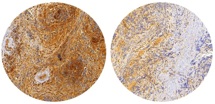
Look at the two histopathological stains below and spot the difference.
High- and low-risk neuroblastoma biopsies. (Courtesy: Rebeca Burgos, Samuel Navarro and Rosa Noguera)
Could you tell which biopsy belongs to a high-risk neuroblastoma patient and which belongs to a low-risk neuroblastoma patient? No? Me neither. But researchers in Spain have combined top-notch image analysis with complex graph theory to identify mathematical features of these images that can help stratify tumours according to malignancy (Int. J. Cancer 10.1002/ijc.32495).
For those of you determined to guess, the high-risk neuroblastoma biopsy is on the left.
The discovery could be particularly helpful in diagnosis of the aggressiveness neuroblastoma, a type of cancer that manifests during the development of the nervous system, most commonly affecting children less than 18 months old. It is difficult to treat and patients suffer widely varying prognoses due to the involvement of many clinical and genetic factors.
The team – led by Rosa Noguera from the pathology department at the University of Valencia-INCLIVA-CIBERONC, and Luis Escudero from the University of Seville and the Seville Institute of Biomedicine-CIBERNED – first took 91 histopathological images from human neuroblastoma and isolated the distribution of a particular glycoprotein known as vitronectin (VN) in the tumour microenvironment. They had previously shown that the arrangement of VN could be connected to tumour progression (BMC Cancer 10.1186/s12885-019-5693-2).
In order to stratify neuroblastoma tumour samples according to patient risk group and the propensity for tumour cell mutation during cell division, the researchers then sought to identify topological parameters to describe the VN network. The network itself may be subdivided into territorial and interterritorial VN, with the former being located very close and within individual cells.
Topology to the rescue
The team extracted a total of 47 features with which to characterize the VN networks using an online image analysis pipeline. A mix of both morphological and topological descriptors defined each feature. The novelty of this approach comes from the inclusion of topological information – a branch of mathematics, familiar to physicists and computer scientists, that handles the preserved quantities of networks under deformation.
After analysing the data, the researchers found a statistically significant correlation between six tensegrity indices; tensegrity being one of the features they derived from the images. The researchers found that lower values of these tensegrity indices were associated with neuroblastoma tissue samples with higher risk and higher genetic instability.
The research team also note the importance of the Euler number in identifying potential neuroblastoma patients. They describe this value as “the number of objects in a sample minus the number of holes within those objects” and observed that a high Euler number per network node, in territorial VN, had statistically significant association with the high-risk patients.
Interdisciplinary teamwork
The techniques and analyses used by the research team were complicated. Fortunately, the upshot of the results is easy to understand: topological and morphological parameters associated with the VN network in histopathological neuroblastoma samples can be related to the aggressiveness of the cancer. The researchers suggest that this might be used to streamline patients prior to treatment.
This work and its potential impact are a clear demonstration of the power of a cross-disciplinary approach to tackling cancer. By combining concepts most at home on the chalkboards of mathematics departments, the researchers have identified patterns in biology.
An infrared frequency comb small enough to fit on top of a table has been used to probe the structure and composition of a complex protein molecule. Scott Diddams at the National Institute of Standards and Technology (NIST) in Boulder, Colorado and an international team of collaborators built their system using a relatively simple laser setup, which can span the entire range of mid-infrared frequencies.
Large biological molecules such as proteins have incredibly complex and intricately folded structures, making them notoriously difficult to study. Typically composed of many thousands of atoms, proteins tend to vibrate and rotate at frequencies associated with mid-infrared light. Probing protein molecules with this light, and then measuring their characteristic absorption spectra, can yield important insights into their compositions, structures, and functionalities.
Such experiments have proven difficult because laser spectroscopy systems currently lack large enough bandwidths in the mid-infrared region to study the full range of protein resonances simultaneously. In addition, it is more difficult to accurately tune sources of mid-infrared light and to accurately detect it, than is the case for visible and near-infrared light.
Regular frequency intervals
Diddams’ team addressed these issues by probing protein molecules with a mid-infrared frequency comb generated using two phase-locked fibre lasers. This creates a series of short, bright pulses at regular frequency intervals across the entire range of mid-infrared frequencies – with the frequency spectrum of the light resembling the teeth of a comb. After interacting with the molecule, the light is detected by photodiodes detectors at a spectral resolution of 0.003 cm-1. Overall, the setup is small and simple enough to fit on a table top.
Diddams and colleagues tested their system on NIST’s monoclonal antibody reference protein. Composed of more than 20,000 atoms, this molecule is used to assess the quality of pharmaceutical treatments. By looking at the molecule’s absorption spectrum using the frequency comb, the team measured characteristic signatures called amide bands. These bands are used by biochemists to determine folding, unfolding and aggregation mechanisms in proteins. The researchers also detected sheet structures within the protein; verifying the results of previous studies that have suggested that chemical groups in the protein are connected in flat arrangements.
The team says that its frequency comb system could be combined with other techniques such as infrared atomic force microscopy to create a table-top system to determine the structure of proteins that would rival those at much larger synchrotron facilities. With further research, their techniques could also be used to store information within molecular vibrations and rotations – offering new technologies for quantum computing.
In autoimmune disorders, such as multiple sclerosis (MS) or type I diabetes, the immune cells that normally protect the body mistakenly attack healthy cells. In MS patients, this immune attack damages the myelin sheath that shields nerve cells in the brain and spinal cord, and in those with type I diabetes, the insulin-producing islets of Langerhans in the pancreas are attacked and eventually destroyed.
Stem cells are known to respond to damaged tissue and modulate the immune response, but trials using stem cells to treat autoimmune disorders have had mixed outcomes. Mesenchymal stem cells get trapped in the filter of the lung vasculature bed, with only 1% reaching damaged tissue. Despite this entrapment, there are some therapeutic effects, which led scientists to believe that these stem cells must release something that acts at the inflamed tissue. Researchers have begun to examine the effect of exosomes – nano-sized bundles of molecular components released from cells.
Exosomes have been examined in cancer and type I diabetes, and now for the first time, researchers from the University of California, Irvine, have shown a neuroprotective capability of stem-cell derived exosomes, and identified players in the exosome mechanism of immune-regulation (ACS Nano 10.1021/acsnano.9b01004).
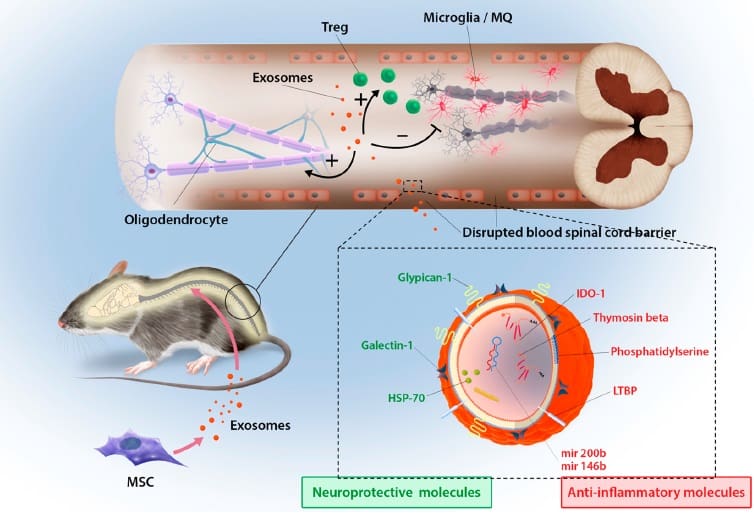
“We showed that due to their size, these vesicles do not get trapped in the lung, and they also target the damaged area and end up into the spinal cord,” says Reza Mohammadi, one of the study’s lead authors.
Interfering with MS
Mohammadi and colleagues used serial ultracentrifugation steps to isolate the (approximately) 115 nm-diameter exosomes from human mesenchymal stem cells the experimental autoimmune encephalomyelitis (EAE) mouse model of MS.
Clinical scoring of the disease revealed improved motor skills and a sustained recovery in exosome-injected mice. And upon dissection, a reduction in de-myelination and regeneration of the protective neural sheaths was discovered.
More potent still was treatment with exosomes released after interferon-gamma stimulation of stem cells. The inflammatory cytokine triggers stem cells and the derived exosomes were shown here to promote neuroprotection in the spinal cord.
Seeking to understand how the exosomes mediated such a neuroprotective response, the scientists delved into the molecular response within the spinal cord. Using a special regulatory T cell reporter model of EAE, a reduction in pro-inflammatory immune cells and a corresponding increase in regulatory immune cells were noted in the spinal cord. In vitro studies confirmed the ability of exosomes to induce regulatory T cells in mouse splenocytes.
Molecular players a plenty
Digging further into the exosome mechanism, Mohammadi performed deep RNA sequencing of exosomes, and identified a plethora of RNA coding for the production of anti-inflammatory proteins. However, using UV light to inactivate exosome RNA in vitro only partially impaired their ability to induce regulatory T cells in mouse splenocyte cultures.
Mohammadi explains that each of the molecules identified could have a wide variety of effects, and work in combination, making it tricky for the team to pinpoint the key players for future enhancement of the treatment.
However, they were excited to identify a potential candidate to explain the increased neuroprotection mediated by interferon-gamma stimulated exosomes. “We observed an upregulation in IDO mRNA and protein – an enzyme potent in inducing T regulatory cells and blocking inflammatory T cell differentiation,” says Mohammadi.
Exosomes vs whole cell therapies
The clinical improvement observed in exosome treated mice was similar in stem cell-treated controls, perhaps indicating that exosomes are the main mediators of stem cell’s immune-regulation and neuroprotection in the spinal cord.
By labelling the exosomes with a dye, the researchers were able to identify that at three hours post injection into EAE mice, some exosomes were located in the inflamed spinal cord. The scientists aren’t yet sure how the exosomes’ targeting system works, although they suspect that inflammation acts as the homing beacon, as no accumulation in the spinal cord was observed in healthy mice.
This work has started to answer some of the burning questions in stem cell therapeutics, but many remain, not least of which is whether nanoparticles will prove more efficacious in human autoimmune disease than whole stem cells. Co-author of the study, Milad Riazifar, will try to find out in the first cell-free exosome clinical trial, scheduled for type I diabetes sufferers in 2020.
What is the most valuable attribute for a laser? Some would argue in favour of efficiency, so that the laser can run off a battery. Others might prefer a device that can turn on and off at high speeds, so it can transmit vast amounts of data. There are also those who place a premium on a circular emission profile, simplifying the focusing of the beam, or argue that what matters most is compatibility with low-cost, high-volume manufacture.
Ticking all these boxes and more is the VCSEL – the vertical cavity, surface-emitting laser. First proposed by Kenicha Iga from Tokyo Institute of Technology in 1977, this class of semiconductor laser is also renowned for its temperature stability, as well as the very low current required to turn it on. Its more common edge-emitting cousin, which is used in CD and Blu-Ray players, long-distance fibre-optic networks, and welding and cutting tools, shares few of these attributes, which is now starting to make electronics manufacturers take notice. Even if you haven’t heard of the VCSEL, there is a good chance that you own a few of them: the iPhone X’s three VCSEL chips play a key role in its facial recognition system. Before iPhones became the killer application, data centres provided the biggest market, with VCSELs deployed in short-reach communication. Both sectors are helping to drive up sales. According to market analyst Yole Développement, global sales revenue reached almost $700m in 2017, and will swell to $3.5bn by 2023.
Sales could go even higher, though, if the VCSEL can expand its spectral range. Today’s commercial offerings are restricted to the red and the infrared. If VCSELs could emit in the blue and green region of the spectrum, they could be used for high-resolution printing, high-density optical data storage, and chemical and biological sensing. What’s more, the combination of red, green and blue VCSELs would make it possible to use these chips in full-colour displays and lighting. Although output power requirements for the VCSEL vary by application, a useful ballpark figure is 10 mW – enough for augmented reality devices, projection systems and displays. The good news is that after more than a decade of hard-fought progress in both industrial and academic labs, this benchmark has now been met for blue VCSELs, thanks to innovations in the device’s architecture and its fabrication processes.
Getting the blues
Given the success of infrared and red VCSELs, the “obvious” road to developing blue and green cousins was to retain as much of their design as possible, while shifting the wavelength. Unfortunately, the “obvious” road turned out to have some considerable bumps.
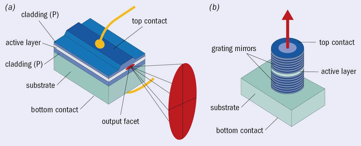
1 Top class: (a) In an edge-emitting laser, the emitted beam is elliptical in shape, making it more challenging to focus and manipulate the beam. (b) In contrast, a VCSEL, which emits from the top of the structure, produces a circular output profile.
Lying at the heart of every laser is its cavity, where light is generated and amplified to produce stimulated emission. This cavity is bookended by a pair of mirrors, providing optical feedback – a prerequisite for lasing. In a VCSEL, the cavity is just a few microns thick, hundreds of times thinner than typical cavities in edge-emitters (figure 1a). Such a short cavity enables the device to turn on and off very quickly, but the penalty is that the mirrors need to be highly reflective for lasing to happen.
The process of making infrared and red VCSELs begins by taking a thin disc of crystalline gallium arsenide (GaAs) and growing on top of it alternating layers of GaAs and (depending on the emission wavelength of the laser) either aluminium arsenide (AlAs) or the alloy aluminium gallium arsenide (AlGaAs). This stack of layers acts as the first mirror. The cavity that contains the light-emitting region is then added, followed by the layers that make up the second mirror (figure 1b). To define precisely where the light comes out of the VCSEL, a circular aperture is constructed by selectively oxidizing, from the outside in, an aluminium-rich layer below the top mirror. The process continues until only a non-oxidized hole, with a diameter of a few micrometres, remains. As this hole is the only part of the layer that can pass a current, the local current density rises high enough for lasing to begin.
A crucial detail of the VCSEL’s construction is that each layer in the mirror stacks must have a thickness equal to one-quarter of the lasing wavelength. This requirement (and the π-phase change that occurs when light reflects off an interface with a higher refractive index material) ensures that all the light that arrives back at the cavity has the same phase, regardless of which part of the mirror provided its reflection. Constructive interference results, supporting lasing of the VCSEL. The pairing of GaAs and either AlGaAs or AlAs is a good one in this respect because the materials’ refractive indices are very different. This means there is substantial reflection at interfaces within the mirror, and 20 or so layer pairs per mirror are enough to reflect 99% of the light.
Unfortunately, the arsenides, which are also used to make countless red LEDs and edge-emitting lasers, are incapable of emitting light at much shorter wavelengths. The obvious solution for making blue and green VCSELs is to replace them with nitrides – the material system used for making blue and green LEDs and edge-emitting lasers. All teams developing blue and green VCSELs have adopted this approach, but it comes with certain drawbacks. In particular, the refractive indices of the nitrides are relatively similar. Getting sufficiently reflective mirrors therefore requires roughly twice as many layers, leading to an unacceptably long time for growing the entire device structure.
Dielectric delights
Recognizing this, Nicolas Grandjean, who heads a group at EPFL, Switzerland, that pioneered nitride VCSELs, chose to replace the top mirror with one formed from a pair of dielectric materials with a significant refractive index contrast. By making this top mirror from a combination of silicon nitride and silicon dioxide, Grandjean and his colleagues trimmed the number of layer pairs in this mirror to just 16.
Even with this modification, fabricating the device is far from easy. That’s partly because the task of growing the bottom, nitride-layer mirror for blue and green VCSELs is more challenging than the equivalent task in arsenide-based devices. Atoms in the crystalline structures of AlGaAs and GaAs are spaced almost the same distance apart, so when one material is grown on the other, there is no build-up of strain in the structure. That’s important, because, left unchecked, strain can generate performance-impairing defects.
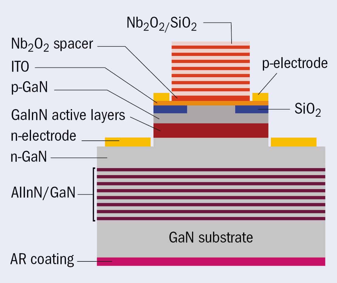
2 More power: Efforts to improve the output power of the nitride VCSEL have spawned many different designs. The one with the highest output power to date is shown here. Produced by a collaboration of researchers at Meijo University and Stanley Electric, it incorporates a bottom mirror (known technically as a distributed Bragg reflector, or DBR) made from alternating layers of aluminium indium nitride (AlInN) and gallium nitride (GaN); a top mirror made from alternating layers of two dielectric materials (niobium oxide, Nb2O5 and silicon dioxide, SiO2); and an active layer of gallium indium nitride (GaInN) grown on a gallium nitride substrate.
To stop strain building up in nitride layers, Grandjean and co-workers paired GaN with the alloy aluminium indium nitride (AlInN), which is lattice-matched to GaN in the form Al0.83In0.17N. Growing a uniform film of this material is not easy, but Grandjean’s team identified conditions for producing good quality AlInN before building their VCSELs. Their design, which has an aperture formed by oxidizing AlInN, also featured a novel approach to injecting current into the device. In a conventional VCSEL, current flows through the mirrors. But dielectric mirrors don’t conduct, so they added electrical contacts to either side of the cavity.
Humble beginnings
The work of Grandjean’s team was carried out more than a decade ago, and the high point came in 2007, when they demonstrated lasing in a blue VCSEL pumped with an argon-ion laser. However, when their VCSEL was driven electrically – the mode of operation required for a practical device – they were only able to extract non-coherent light from it. Further progress would have required additional refinements to the fabrication processes, but funding for such work was unavailable in part because decision-makers argued that the necessary breakthroughs would come via work being done in Japan, where researchers pioneered light-emitting nitride devices in the 1990s.
Broadly speaking, they were correct: much of the subsequent progress in VCSEL development has indeed come from scientists at Japanese electronics firms. However, other groups have also made valuable contributions. Among them is a team from National Chiao Tung University, Taiwan, which reported the first electrically driven nitride VCSEL in April 2008. To coax laser light out of their device, the researchers cooled it with liquid nitrogen. This is not practical for a commercial light source, but further progress came later that year when researchers at the Japanese firm Nichia produced the first blue VCSEL capable of operating at room temperature. Appropriately enough, Nichia is where Shuji Nakamura, who shared the Nobel Prize for Physics in 2014 for developing blue LEDs and is also credited with inventing the blue laser diode, spent much of his career.
Nichia’s design broke new ground, dispensing with nitride mirrors altogether. However, it’s debatable whether this made its VCSEL easier to fabricate. After the cavity was grown, it had to be removed from the substrate that provided the foundation for its growth and then carefully polished to a very precise thickness, defined by the lasing wavelength. Despite this, Nichia persisted with the design, and in 2009 engineers announced that they had increased the laser’s output from 0.14 mW to 0.62 mW by switching the substrate from sapphire to GaN. This change improved material quality, slashing defects by three orders of magnitude.
Unfortunately, the Nichia team also found that after just 10 minutes of operation, the minimum current needed to turn on their devices started to drift – perhaps because of mechanical stress induced in the GaN wafer during the polishing process. The company reported a modest improvement in the output power of its blue VCSEL in 2011, but it has not published any papers on this topic since 2012, suggesting that its process has significant issues.
Milliwatt milestones
It took several years, and yet more innovation, to produce the first VCSEL with an output power of 1 mW or more. Sony claimed this milestone in 2016 with a 1.1 mW blue VCSEL produced with a process that begins by forming islands of dielectric mirrors, before growing GaN material between and then over them, and finally depositing the cavity. After this, a second dielectric mirror is added.
More recently, Sony’s engineers unveiled a new design that has broken the 10 mW barrier. It features a far larger cavity and a curved mirror, formed by etching the backside of the substrate and depositing a dielectric stack on this surface. In November 2018 team spokesperson Tatsushi Hamaguchi announced that they had achieved an output power of 12 mW for their blue-emitting VCSEL. At the Photonics West conference in San Francisco, US, a few months later, Hamaguchi revealed a further increase, to 15.4 mW.
Sony’s high-power design has competition in the form of a blue-emitting VCSEL based on an architecture that shares several features with EPFL’s early work. In 2017 researchers at Meijo University and Nagoya University in Japan used a dielectric top mirror and a bottom mirror containing AlInN to construct a VCSEL with a 4.3 mW output. They reported their progress at the International Workshop on Nitride Semiconductors in Strasbourg, France, and Grandjean, of EPFL, called it an impressive result. “The secret is with the growth conditions,” he says. “They can grow at a high temperature and faster, so they improve both the quality of the material and the growth time.”
Since then, Tetsuya Takeuchi and his team from Meijo University have partnered with engineers at Stanley Electric, a Japan-based electronics firm that supplies headlamps to car manufacturers such as Honda and Nissan. Their goal is to increase output power still further, so that Stanley can replace the LEDs in its headlamps with VCSELs. In early 2018 the partnership revealed that it had hit 6 mW by trimming internal loss, and in autumn of the same year the scientists reported that they had exceeded 15 mW by lengthening the cavity and quashing thermal resistance. The latest figure in the public domain is 22.2 mW, announced at the 2019 Photonics West, where team members attributed the increase in power to having optimized the reflectivity of the top mirror.
It’s not easy being green
Replicating these advances for green VCSELs has so far proved difficult. In blue and green LEDs and edge-emitting lasers, light is generated in very thin layers of InGaN, known as quantum wells. Green emission requires more indium in the wells, but this increases the strain, generating defects and impairing performance. Compounding matters, the in-built electric field in this material system increases in strength with indium content, hampering the light-generation process.
To sidestep these issues, a partnership in China between researchers at Xiamen University and the Chinese Academy of Sciences, Suzhou, has turned to quantum dots. The advantages of this move, which include reductions in strain and internal electric field strength, have enabled the fabrication of VCSELs that span the entire green spectral range. So far, the output powers are lagging their blue siblings. However, with the latter now on the cusp of commercialization, funding for green GaN VCSELs is sure to grow, spurring this impressive light source to span a wider spectral range and serve even more applications.
Enjoy the rest of the 2019 Physics World Focus on Optics & Photonics in our digital magazine or via the Physics World app for any iOS or Android smartphone or tablet.
Physics World’s Laser at 60 coverage is supported by HÜBNER Photonics, a leading supplier of high performance laser products which meet the ever increasing opportunities for lasers in science and industry. Visit hubner-photonics.com to find out more.
Researchers have put forward a completely new heat transport mechanism – known as chiral zero sound – in Weyl semimetals. The new mechanism could explain recent observations of higher-than-predicted oscillations of the thermal conductivity in these materials along the direction of an applied magnetic field and may even be exploited to control the thermal current through certain types of electronics devices using this field.
A Weyl semimetal is a recently discovered class of topological material (one that can be insulating in the bulk but has conducting surface states due to symmetry-protected topological order). In these materials, electronic excitations behave as massless, Weyl, fermions. These particles were first predicted in 1929 by the theoretical physicist Herman Weyl as a solution of the Dirac equation.
The chiral magnetic effect
Fermions that can be described by Weyl’s theory can appear as quasiparticles in solids that have linear electron energy bands crossing at (Weyl) points near the Fermi energy. These quasiparticles behave quite differently to electrons in ordinary metals or semiconductors in that they show the chiral magnetic effect (CME). This occurs when a Weyl metal is placed in a magnetic field, which generates a current of positive and negative Weyl particles that move parallel and antiparallel to the field.
The net current flow is usually zero because the positive and negative particles are present in equal amounts. This thermodynamic balance changes, however, when an electric field is applied parallel to the magnetic field. In this case, a net quasiparticle current flows and this effect, known as the chiral anomaly, can manifest itself as negative magnetoresistance – a lowering of the resistance with increasing magnetic field.
Zero sound is a quantum mechanical effect first put forward by the theoretical physicist Lev Landau in the context of Fermi-liquid theory. Like normal sound, zero sound comes from vibrations, but instead of being carried by air molecules, the vibrating medium in the case of zero sound is in fact the momentum distribution of electrons near the Fermi Level.
The Hong Kong team has now indeed shown that these zero sound vibrations exist in Weyl semimetals when a magnetic field is applied and that they significantly contribute to the material’s thermal conductivity. The chiral sound wave is quite different to the zero sound proposed by Landau though because it is an electronic acoustic mode and only propagates along the applied magnetic field direction, says Dai. “What is more, we can strongly modulate its velocity using the magnetic field, which is quite exotic because only the thermal conductivity parallel to the field oscillates.”
The researchers say that the CZS described in their work could be directly measured in various types of experiments. These include: by a pump and probe optical measurement technique; by detecting the possible formation of polariton modes (quasiparticles that are part matter and part light) formed by the hybridization of CZS and optical phonon modes (vibrations of the crystal lattice); and by using supersonic measurements.
“Completely new sound mode”
“We have proposed a completely new sound mode carried by Weyl fermions under a magnetic field,” Dai tells Physics World. “Until now, we could only ‘see’ these fermions using techniques like angle-resolved photoemission, but now we could also ‘hear’ them.”
Since, the CZS can conduct thermal current only along the direction of the applied magnetic field, it might be exploited in some special devices that would allow us to control thermal current flow using a magnetic field, he adds.
The researchers say they established the basic theory of CZS in a previous paper but they still need to perform quantitative calculations for the CZS velocity for each particular Weyl semimetal they have studied. “We have some clear ideas on how to conduct the first principles calculations for calculating this velocity and have already begun related computational work,” reveals Dai.
A graphene-based desalination membrane with the potential to be scaled-up for practical applications has been created by a team of physicists in China and the US. Yanbing Yang and Xiangdong Yang at Wuhan University and colleagues created the material by combining a single sheet of graphene with a mesh of carbon nanotubes to create a centimetre-sized membrane that can remove salt from seawater.
As the demand for fresh water increases worldwide, large-scale, new technologies for the desalination of seawater are becoming increasingly sought after. Removing salt from water is easily done by evaporation, but this requires large amounts of energy. Today, most modern plants pump seawater through a membrane that blocks the passage of salt ions. Called reverse osmosis, this process requires less energy than evaporation but could benefit from better membranes.
The answer could be to use graphene, which is a sheet of carbon just one atom thick. Graphene is very strong, and sheets can be punctuated with sub-nanometre-sized pores that let water through while blocking salt. While this works well for micrometre-sized membranes it is very difficult to make larger graphene sheets without defects, which act as large pores that let salt through. Defects also reduce the mechanical strength of the graphene, making it difficult to create larger membranes.
Another approach is to create a membrane from a patchwork of small overlapping sheets of graphene oxide (also just one atom thick). Water can move through the membrane by permeating the gaps between the sheets – but the larger salt ions cannot. While scientists have already made centimetre-sized membranes this way, this material tends to swell-up when wet and let more salt through.
Mesh-like network
In this latest research, Yang, Yang and colleagues have devised a way to create centimetre-sized sheets of porous graphene that do not suffer from the effects of defects. This was done by depositing a mesh-like network of single-walled carbon nanotubes on top of a graphene sheet, which essentially reinforces the material and blocks the spread of cracks and tears. Then the pores are etched in the material to create a desalination membrane.
When tested, the team’s membranes could remove between 85-97% of salt from seawater. While this is impressive for such large membranes, it would have to be boosted to greater than 99% to be used in commercial desalination systems. The team says that scaling the membrane up to metre sizes should not be a problem.
A possible next step in creating practical large-scale membranes could be to stack several layers of nanotube-reinforced graphene membranes on top of each other. Molecules would enter the membrane via a pore but would then have to travel some distance between layers to find a pore in the next layer. This would mitigate problems associated with the widening of pores in single layers, and the presence of pores would minimize the swelling of the membrane.
The study suggests that any long-term changes in atmospheric rivers could impact sea-level variation along the coast.
Toshiaki Shinoda at Texas A&M University, US, and colleagues demonstrated that atmospheric rivers above the US west coast affect the ocean and fluxes between the ocean and atmosphere. The south-westerly winds associated with these atmospheric rivers, they found, generate surface ocean currents that pile up water along the west coast of North America, rapidly increasing sea level.
Atmospheric rivers are relatively long and narrow regions of the atmosphere that often release water vapour as precipitation when they move from above the ocean to the land. The most well-known is the “Pineapple Express”, which transports moisture from the central Pacific to the west coast of the US.
The two atmospheric river events analysed during CalWater 2015. Total column integrated water vapour (mm) on (a) January 16, and (b) February 6, 2015 derived from Special Sensor Microwave Imager (SSMI) data. The circle and triangle indicate the locations where sea level was measured. (Image courtesy: Scientific Reports and Toshiaki Shinoda et al)
Research on these “rivers in the sky” has increased over recent years as their importance for global water transport has become apparent; they’re responsible for most of the poleward water vapour transport at middle and high latitudes as well as extreme weather such as heavy precipitation.
Shinoda and colleagues examined two strong atmospheric river events observed during the 2015 field campaign for the CalWater Precipitation, Aerosols and Pacific Atmospheric Rivers Experiment. They used data products including high-resolution ocean reanalysis and tide gauges.
To complement these case studies, the researchers analysed a dataset of 1584 atmospheric river events in the northeast Pacific from 2011-2015. This established that the oceanic processes found in the CalWater 2015 case studies are found in most atmospheric river events.