Two researchers in Poland have used neural algorithms to transform photographs into the style of cartoon drawings. Maciej Pesko and Tomasz Trzcinski at Warsaw University of Technology used several different state-of-the-art “style transfer” and “instance normalization” algorithms to convert a selection of photographs into ten different illustrative styles – including a Spider Man comic, Mickey Mouse cartoon and the iconic Japanese print The Great Wave off Kanagawa.
Pesko told me that their work has several aims including generating images in painting styles of famous artists; rendering similar textures in computer games; changing image scenery (from day to night, for example); and face swapping.
They describe their technique in a preprint on arXiv and they have set-up a website for “comixifying”. The above comixified image was created from a photo of a jumping horse and rider and there are many more examples in the preprint.
Researchers in Japan have created a long-lasting magnetic field with a strength of 1200 T, which is the strongest controllable field ever produced indoors. In comparison, Earth’s magnetic field is a mere 50 μT and the superconducting magnets on CERN’s Large Hadron Collider deliver about 8 T.
Daisuke Nakamura and his team at the University of Tokyo fine-tuned the technique of electromagnetic flux-compression (EMFC) to achieve the result. Their work could allow for new experiments in solid-state physics and could even boost the performance of nuclear fusion reactors.
Extremely strong magnetic fields are useful for probing the physics of materials. However, creating and maintaining extremely strong fields is notoriously difficult to do. High-power lasers can be used, but this results in fields that last for just nanoseconds.
Another strategy involves first generating a relatively strong field in a metal cylinder (called a liner) by surrounding it with a magnetic coil. By suddenly imploding the liner, the magnetic field it contains is compressed to reach very high strengths.
Explosive technique
Physicists have developed two ways of causing the implosion. One is explosively-driven flux-compression, which use chemical explosives such as TNT. In 2001, physicists in Russia achieved a field strength of 2800 T with this method. However, they had virtually no control over the field during the experiment, and their setup was destroyed. Furthermore, these explosive experiments must be done outdoors.
Alternatively, EMFC exploits the vast amounts of electrical energy that can be stored inside a bank of capacitors. The liner is surrounded with a specialized-designed coil that is connected to the bank. The capacitors then release a huge current of four million amperes, which is hundreds of times the current of a typical lightning bolt. This induces a strong magnetic force acting inwards towards the axis of the liner – driving a clean and precise implosion. Despite an impressive shower of sparks (see figure), the technique can be carried out safely inside a lab.
Nakamura’s team has been at the forefront of efforts to perfect EMFC technique by tweaking the arrangements of coils and capacitor banks. Indeed, they achieved a field strength of 985 T earlier this year. Yet with further optimization of their setup, the researchers have now delivered a record-breaking indoor field strength of 1200 T. What is more, their field lasted for around 100 µs– thousands of times longer than previous ultra-high fields.
Plasma confinement
“With magnetic fields above 1000 T, you open up some interesting possibilities. You can observe the motion of electrons outside the material environments they are normally within, so we can study them in a whole new light,” comments Nakamura’s colleague Shojiro Takeyama. “This research could also be useful to those working on fusion power generation by confining plasma in a large ring called a tokamak to extract energy from it. This requires a strong magnetic field in the order of thousands of Tesla for a duration of several microseconds. This is tantalizingly similar to what our device can produce.”
Nothing brings people together like a crisis, and there can be no crisis like the end of the world. Last week, researchers from all over the world came together at the University of Surrey to exchange ideas at the Advanced Energy Materials 2018 conference. Following some stern stats in the plenaries of the brutal pace of catastrophic climate change, the building was awash with ideas and developments for alternative energy generation and storage technologies. “For clean energy we need more than one solution,” said John Zhu, from the University of Queensland in Australia. While his own presentation focused on solid-oxide fuel cells, he emphasized how fue- cell and battery research can complement each other. Similarly, many of the researchers attending the meeting had potential collaborations at the top of their agenda for the conference.
Of course, not all energy materials research is motivated by the harm caused by fossil fuels, and while scientific meetings and conferences continue to multiply, most of them have little or nothing to do with a pending climate-change-induced global apocalypse. However, the urge to collaborate remains a common thread, allowing researchers to pool resources and find new space for discovery that weaves together different strands of expertise.
If the number of scientific conferences seems to be growing, the number of journals housing peer-reviewed research seems to be breeding at the rate of bacteria in a petri dish, and like bacteria some of these new journals could prove vital for the health of the communities they serve. The recently launched Journal of Physics: Materials, which published its first papers this week, is aiming to be one of those journals the field can’t live without, and some of the reasons include collaboration and cross-fertilization.
“Actually the emergence of new journals is a bit impressive and overwhelming – and we see that journals are focusing more and more on a narrower scope,” said ICREA Professor and Journal of Physics: Materials Editor-in-Chief Stephan Roche in an interview with Physics World. “Journal of Physics: Materials on the contrary wants to emphasize the quality of the science but wants to keep a large landscape so that we have a platform where advances in novel materials or the foundation for technologies will knit together and inspire other authors publishing in the journal to collaborate.”
So far the claim does not seem an empty aspiration. Discussing just a handful of the papers in the first issue revealed a ripe opportunity for collaboration between authors of two of the papers reporting results from graphene-based research, and with so many developments cropping up at the interface of different disciplines, there may be more interesting work to come from authors of less obviously associated papers teaming up.
You can find coverage of some of the energy storage research presented at Advanced Energy Materials 2018 as well as some of the highlights from the first issue of Journal of Physics: Materials including graphene plasmon device research and nanoscale polymer LED fabrication in the materials section of Physics World.
A nanoscale polymer LED device fabricated on a polyethylene terephthalate (PET) substrate using adhesion lithography.
Potential applications of nanoscale polymer LEDS abound, but efficient nanofabrication methods to produce them remain limited. Reporting in the first issue of the Journal of Physics Materials, Thomas D. Anthopoulos and colleagues at Imperial College London and the National Physical Laboratory in the UK, and King Abdullah University of Science and Technology (KAUST) in Saudi Arabia show how the recently developed adhesion lithography technique enables the versatility and precision to produce high-performing polymer green-light-emitting diodes with an inter-electrode distance of under 15 nm and an aspect ratio of up to 106.
As well as potential light sources for scanning near-field optical microscopes and nanoscale photopatterning, the efficient dissipation of Joule heating allows nanoscale polymer LEDs to achieve higher current densities that may eventually enable electrically pumped organic lasers. Yet as Anthopoulos and co-authors point out in their report, “Further progress has, however, been hindered by manufacturing challenges, as shadow masking and conventional photolithography cannot produce nanometre-sized electrode features between different metals, while e-beam lithography is not suitable for upscale while it is often limited to a single electrode material.”
Adhesion lithography brings versatility
Alongside researchers at Imperial College London and KAUST, Anthopoulos described how adhesion lithography could produce nanogaps less than 15 nm apart between electrodes of different materials in Nature communicationsin 2014 . The approach involves depositing a self-assembled molecular layer on a pre-patterned metal layer, thereby weakening its adhesion to a subsequently deposited metal layer. They then exploited the weakened adhesion to remove the second metal layer from the first with tape, leaving the second layer only in the prepatterned gaps of the first metal, and a nanogap between the two metals once the self-assembled molecular layer is removed.
Anthopoulos and colleagues now apply the technique to fabricate nanoscale polymer LEDs with one gold and one aluminium electrode and the light emitting polymer poly(9,9-dioctylfluorene-alt-bithiophene) (F8T2). The ability to fabricate the LED with different metal electrodes allows them to engineer preferential hole injection from the gold Fermi level to the F8T2, since the potential barrier is lower than at the interface between F8T2 and aluminium.
Redshifts in the photoluminescence specra compared with F8T2 on quartz indicate the effects of nanoconfinement of the polymer in the nanogap. They also demonstrate improved light output from the LED by increasing the aspect ratio, as well as devices fabricated on plastic and glass.
“To the best of our knowledge this is the first example of a flexible nano-PLED fabricated on a plastic substrate. The consistency of these results with the ones obtained on glass substrates demonstrate the versatility of a-Lith to create large size nano-gap devices on a variety of substrate materials,” say Anthopoulos and co-authors in the report.
ICREA Professor Stephan Roche, who is Editor in Chief of the Journal of Phyiscs: Materials, and not involved with the current research highlights the significance of demonstrating the fabrication technique on plastic and glass. “If you base your technology on silicon only and you want to miniaturize, the cost increases more and more as you narrow down the size of the device. In this case glass and plastics are very common materials, the cost is very low and their technology is chemically driven so it doesn’t really add an additional cost. Instead it brings versatility, complexity in terms of the possible architectures, and it brings a light source at the nanoscale – that’s a new dimension for a lot of applications.”
Pancreatic phase images reconstructed with FBP and ADMIRE. The arrow indicates the location of the GTV. (Courtesy: L D Di Maso et al/CC BY 4.0)
Pancreatic adenocarcinoma typically has a poor prognosis, and while surgery can cure some cases, 80% of patients with pancreatic cancer are not surgical candidates. Radiation therapy offers an alternative treatment option, but contrast between pancreatic tumours and surrounding healthy tissue is low, making target delineation and treatment planning a challenge.
To address this challenge, a team from the University of Wisconsin-Madison has investigated the ability of split‐filter dual‐energy CT (DECT) to improve pancreatic tumour contrast and contrast‐to‐noise ratio (CNR) for radiotherapy planning. The researchers used the new TwinBeam modality on the SOMATOM Definition Edge CT scanner to image 20 patients with pancreatic adenocarcinoma (J. Appl. Clin. Med. Phys.19 676).
DECT uses two different photon energies to image patient anatomy, enabling differentiation of tissues with similar density but different composition. TwinBeam utilizes a split‐filter to spatially separate a helical 120 kVp X‐ray beam into a low‐ and a high‐energy beam. Scans can be reconstructed as mixed 120 kVp‐equivalent images, which mimic conventional single‐energy images, or as virtual monoenergetic images (VMIs) with energies ranging from 40 to 190 keV.
Each patient in the study was injected with the iodine contrast OMNIPAQUE, and all but one underwent both pancreatic and portal venous phase scans. For each phase, the researchers reconstructed the raw data using two methods: filtered back projection (FBP) and an iterative reconstruction algorithm called ADMIRE.
To determine the energy that produced the greatest contrast and CNR, the researchers first reconstructed VMIs at 5 keV increments. They found that the 40 keV VMI produced the greatest CNR for pancreatic tumours and used this energy for further studies, along with the VMI at 57 keV, which was chosen based on physician initial preference.
Image analysis
To assess differences in contrast and CNR between the reconstructed datasets, the researchers defined three regions-of-interest (ROIs): the gross tumour volume (GTV); an ROI within healthy pancreatic tissue near the GTV; and an ROI in the erector spinae muscle to assess image noise.
The mean GTV contrast for pancreatic phase images reconstructed using FBP was 15.9 HU for mixed 120 kVp‐equivalent images, 40.7 HU for 57 keV VMIs and 93.7 HU for 40 keV VMIs. For FBP-reconstructed portal venous phase images, the mean GTV contrast was 6.01, 16.4 and 41.5 HU, for the mixed 120 kVp‐equivalent images, 57 keV VMIs and 40 keV VMIs, respectively.
The authors note that, on average, images reconstructed with ADMIRE had slightly greater contrast, but that the improvement was not statistically significant.
Noise in the VMIs increased with decreasing energy, as expected. Averaged over the pancreatic and portal venous phase datasets (which exhibited similar noise levels), the mean image noise was 13.2 HU for mixed 120 kVp‐equivalent images, 20.3 HU for 57 keV VMIs and 28.0 HU for 40 keV VMIs. The use of ADMIRE iterative reconstruction reduced noise to 10.6, 15.8 and 22.2 HU for the respective images -- a decrease of about 20% throughout.
Contrast‐to‐noise ratio for pancreatic and portal venous phase scans, reconstructed with FBP or ADMIRE. (Courtesy: L D Di Maso et al/CC BY 4.0)
Finally, the researchers calculated the CNR for the six datasets. The mean CNR in the GTV for pancreatic phase images reconstructed with FBP was 1.37, 2.41 and 3.86, for mixed 120 kVp‐equivalent images, 57 keV VMIs and 40 keV VMIs, respectively. ADMIRE further improved the CNR for all cases, increasing to 4.94 in the 40 keV VMIs.
They note that DECT images acquired in the pancreatic phase demonstrated greater GTV contrast and CNR than those acquired during the portal venous phase, suggesting that the pancreatic phase is superior for tumour delineation.
The authors conclude that VMIs reconstructed using split‐filter DECT significantly improved pancreatic tumour contrast and CNR compared with virtual single‐energy CT images, and that iterative reconstruction further improved CNR. This contrast gain may lead to more accurate tumour delineation for radiotherapy planning, potentially leading to more effective treatment.
Simple solutions are often the best, and British and European climate scientists have identified one: forests cut warming better than the technological solutions now being widely canvassed.
They have established some simple ground rules for limiting global warming to the international target of an average rise of no more than 1.5 °C by 2100.
Rule one: do not try to generate electric power with biofuels made from harvested crops, trees or grasses, and do not spend even more money trying to capture the carbon dioxide emissions, liquefy them and bury them deep underground. To do so successfully would require at least 380 million and maybe up to 700 million hectares of farmland.
This is about half of the space already needed to grow food for more than 7 billion humans.
Rule two: do preserve and regenerate the world’s forests. They already capture the greenhouse gas carbon dioxide and preserve it as root and branch. Yet more intact forest would be even more effective.
“The vast majority of IPCC scenarios for how we can limit global warming to less than 2 °C include BECCS,” said Anna Harper, a mathematician at the University of Exeter in the UK. “But the land required to grow biomass in these scenarios would be twice the size of India.”
She and colleagues report in the journal Nature Communications that they used a computer simulation of the world’s vegetation and soil and tested it with a series of scenarios that might keep global average temperatures to either 2 °C or 1.5 °C above pre-industrial levels. Since the start of the Industrial Revolution two centuries ago, global average temperatures have already risen about 1 °C.
The computer models delivered an answer: to switch to crop biomass and carbon capture on a global scale would actually lead to an increase of carbon in the atmosphere, to ramp up global warming even further, and precipitate what could be, for many, catastrophic climate change.
The researchers don’t dismiss the biofuel technology entirely: in some cases it might be an effective solution. But, overall, it would be better simply to protect and restore the world’s forests.
Biofuels – generated from fields of sugar cane, maize, trees or grasses such as miscanthus – are already big agribusiness, but both environmental campaigners and climate scientists are concerned about their effectiveness in reducing greenhouse gas emissions and about their potential impact on food prices.
“To meet the climate change targets from the Paris Agreement, we need to both drastically reduce emissions and employ a mix of technologies to remove carbon dioxide from the atmosphere,” said Harper. “There is no single get-out-of-jail-free card.”
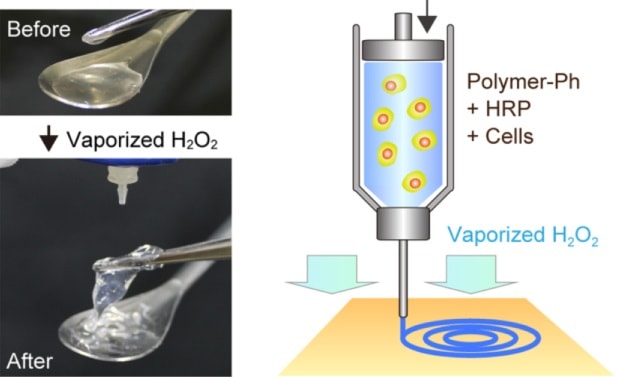
An airborne technique forms hydrogels after extrusion, preventing blockages within the needle
Researchers in Japan have devised an improved technique for producing the cell-laden hydrogels, or “bioinks”, that are crucial for 3D bioprinting (Biofabrication 10 045007). The technique can form hydrogels within just six seconds and, when used with a micro-extrusion device, can create 3D hydrogel constructs in which 90% of the live cells survive the fabrication process.
The researchers have re-invented an established technique in which an enzyme called horseradish peroxidase (HRP) is used to catalyse the cross-linking of various polymers to form hydrogels. Bioinks produced by this enzymatic reaction are often used in extrusion-based bioprinting – the most widely studied to date – in which the hydrogel is forced through a syringe or a printer-head nozzle and then quickly stabilized to produce a fixed, printed structure.
The technique is popular because it does not harm the live cells encapsulated within the hydrogel, plus it enables a variety of polymers to be used as the bioink. One problem, however, is that the reaction requires HRP to be mixed with hydrogen peroxide (H2O2), which is usually done in an aqueous solution. Once these mixtures are loaded into a syringe for subsequent printing, the HRP-catalysed reaction starts to form cross-links almost immediately – which can clog and plug up the needle.
Air replaces water
The new technique, developed by Shinji Sakai and colleagues of the Graduate School of Engineering Science at Osaka University, overcomes this problem by supplying hydrogen peroxide as a gas. By passing air through an aqueous solution of hydrogen peroxide, the researchers created an airflow that was rich in hydrogen peroxide. Extruding the bioink into this airflow catalyses the HRP reaction and allows the hydrogel to form.
“We prepared our hydrogels by contacting air containing between 10 and 50 ppm H2O2 with an aqueous solution filled with polymers comprising phenolic hydroxyl (Ph) groups and horseradish peroxidase,” explains Sakai. “In this system, HRP catalyses cross-linking of the Ph groups by consuming the airborne H2O2.”
According to Sakai, the researchers can tune the hydrogelation rate and mechanical properties of the resultant hydrogels by controlling the concentration of hydrogen peroxide in the air, the exposure time of the bioink to the airflow, and the HRP concentration in the bioink.
The airborne technique, which the researchers report in the journal Biofabrication, can be used in a micro-extrusion device containing bioinks made up of HRP, polymer(s) cross-linkable by HRP, and biological cells. “These bioinks are extruded into air containing H2O2 and cross-link though the HRP enzymatic reaction,” Sakai tells Physics World. “They gel immediately after contacting with air.”
Sakai and colleagues proved that the hydrogels were biocompatible by enclosing mouse fibroblast cells inside the structures. 90% of these cells survived and, what is more, successfully spread throughout the hydrogels.
A variety of polymers can be cross-linked through the HRP enzymatic reaction, and the researchers say that they would now like to develop cell-laden 3D hydrogel constructs using multiple bioinks. “These could contain different types of cells and different polymers for fabricating functional 3D tissue,” explains Sakai.
Read our special collection “Frontiers in biofabrication”to learn more about the latest advances in tissue engineering. This article is one of a series of reports highlighting high-impact research published in Biofabrication.
Just 45 quintillionth of a second (45 attoseconds) is all it takes for a photon to liberate an electron from the surface of a metal. That is the conclusion of Joachim Burgdörfer from the Technical University of Vienna and colleagues, who have done a clever sequence of experiments to make the most precise measurement ever of the duration of photoelectric emission. Their technique promises to provide new information about how electrons behave in materials and could lead to improvements to photoelectric technologies, such as solar cells and optoelectronic telecoms components.
Albert Einstein may be most famous for his theories of relativity, but he bagged the 1921 Nobel Prize for Physics for his work on the photoelectric effect. Einstein had worked out why light incident on the surface liberates electrons – but only if the frequency of the light is above a certain threshold. He explained this phenomenon by assuming that light exists as discrete particles (later called photons) in what an important early contribution to the development of quantum mechanics.
As the photoelectric effect occurs so fast, physicists used to think the emission time is too short for them to measure with any precision. But thanks to the development of shorter and shorter laser pulses, they have been encouraged to try to measure the emission time using an "attosecond streak camera". This involves firing two successive ultrashort laser pulses at a material, with the first ejecting an electron and the other accelerating it towards a detector.
The problem with this technique is that, for most materials, it cannot determine the time it takes for one electron to be emitted, although if two electrons from different electronic states are liberated by the first pulse, the time delay between the emissions can be determined.
Atomic “clocks”
Burgdörfer and colleagues have now developed a new technique that uses iodine and helium atoms as “clocks” to measure the absolute time for electron emission from tungsten metal. The method involves depositing iodine atoms on a tungsten surface and using an attosecond streak camera to measure the delay between the emission of electrons from tungsten and emission of electrons from iodine. A second streak-camera measurement is then made on a gas containing iodine and helium – giving delay between electron emission from iodine and helium.
Helium is used because it is a very simple atom, having just two electrons. This means that, unlike tungsten and iodine, the absolute emission time can be calculated from streak-camera data.
Working back via the iodine measurements, the team calculate that tungsten emission times range from about 45 attoseconds for conduction electrons to about 100 attoseconds for electrons in the inner shells of the tungsten atom. Analysis of the times for several different electron states in tungsten, suggests that the emission process is more complicated than previously thought.
"[The technique] gives us the opportunity to study important physical processes with an accuracy that would have been inconceivable a few years ago”, says Burgdörfer. “It is an exciting field of research that provides remarkable new insights – for example into surface physics, and into electron transport processes inside materials.”
In this episode of the Physics World Weekly podcast we talk about an X-ray detector that you can wrap around your finger; new computing technologies that are giving physics a boost; and how to minimize flooding risk during tropical storms. We also take a fresh look at quantum noise in a round-up of what is new on Physics World this week.
If you enjoy what you hear, then you can subscribe via the Apple podcast app or your chosen podcast host.
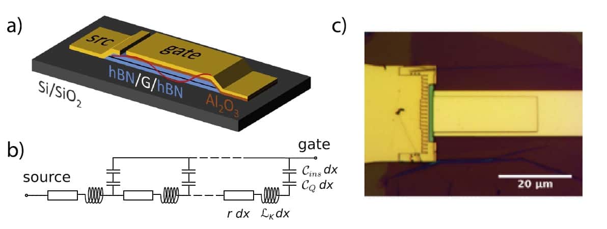
A graphene plasma resonance capacitor. (Credit: Journal of Physics: Materials)
Graphene plasmonics has been caught between a rock and a hard place, with high-energy plasmons readily coupling into hybrid modes, while low-energy plasmons are prone to damping. Now researchers in Japan, Germany and Singapore report in the first issue of Journal of Physics: Materials how they can protect low-energy plasmons from damping by encapsulating the graphene in hexagonal boron nitride (hBN). What is more, in the same issue another group of researchers demonstrate a transfer-free process that could enable mass-production of high-quality hBN-encapsulated graphene devices.
Not high energy proves no great loss
Plasmons – the collective excitations that couple the electromagnetic fields associated with incident light to the electrons in a material - have long attracted interest for potential applications including high-sensitivity sensing and information processing. Graphene plasmons hold the additional allure of being tunable, but so far it has been difficult to produce graphene plasmons that remain uncoupled to surface modes, which form hybrid plasmon-polaritons, while avoiding ohmic losses.
“Tunability is always interesting because then you can really have a recipe, which tells you not just how to generate a property, but also how to switch it on and off,” says ICREA research professor Stephan Roche, editor-in-chief of Journal of Physics: Materials in his discussion of some of the papers in the first issue.
By encapsulating high-quality exfoliated graphene in hBN Bernard Plaçais at Sorbonne University in France and his collaborators produce devices where the graphene plasmons are both very weakly coupled to any other source and have a high Q factor. They demonstrate the approach in plasma resonance capacitors with a 100 μm quarter-wave plasmon mode, at 40 GHz, and a quality factor of around two.
“Our capacitor GHz experiment constitutes a first step toward the demonstration of plasma resonance transistors for microwave detection in the sub-THz domain for wireless communications and sensing,” they point out in their report. “It also paves the way to the realization of doping modulated superlattices where plasmon propagation is controlled by Klein tunnelling.”
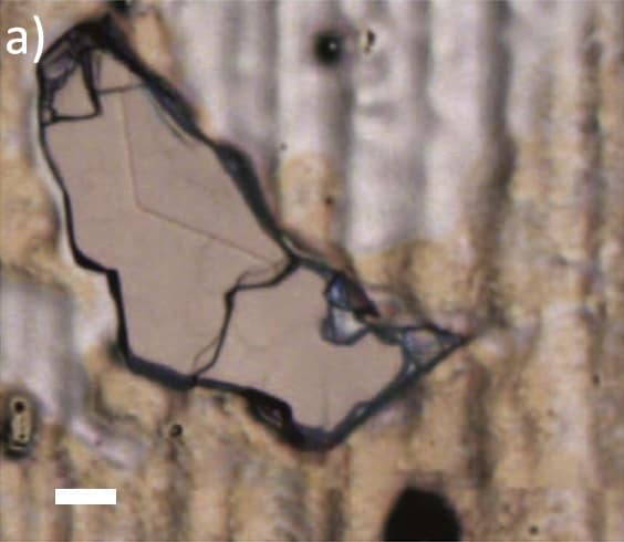
Optical micrograph of a large h-BN crystal exfoliated on a copper foil, fully covered with graphene after the growth. Credit: Journal of Physics: Materials
As with the work by Plaçais and colleagues, when researchers want to show how to exploit graphene’s unique optoelectronic properties in a given device, the preferred graphene fabrication technique is exfoliation, where individual layers are stripped of pristine graphite. However – production scale limitations aside - transferring exfoliated layers of graphene onto hBN inevitably introduces defects, which impinge on the device performance. Instead by growing the boron nitride and then the graphene together without changing the growth parameters Bouchiat and his team show that they can produce high-quality large-area encapsulated graphene with a charge carrier mobility that reaches 2.0 × 104 cm2V-1s-1.
“These two papers are very illustrative of the challenges of research in 2D materials,” says Roche, who was not involved in either piece of research. “On one side you have the forefront of research trying to get really high-quality research devices, and then trying to explore what is unique about these 2D materials, and to demonstrate that they can really bring high value in terms of applications. Then on the other side you have people making efforts to integrate these materials and to upscale their growth so that they can be practical for industries in the medium term.”
Whether the potential of the reported CVD approach can provide mass production of the graphene plasmonic devices remains to be seen. Full details of both reports are found in Journal of Physics: Materialsissue 1.