As demand for this formerly niche type of semiconductor laser rises, companies making the vacuum systems and thin-film process equipment used in their manufacture need to adapt, says Ajit Paranjpe

Vertical cavity surface-emitting lasers, or VCSELs (pronounced “vixels”), were invented in the late 1970s and have since made their way into consumer devices such as computer mice and laser printers. Now, however, rocketing demand for 3D image sensing is pushing VCSELs into new territory, with applications emerging in smartphones, autonomous vehicles and more. Ajit Paranjpe is a senior vice president and chief technology officer at Veeco, a US-based maker of equipment used for thin-film manufacturing processes in the hi-tech electronics sector. He spoke to Physics World about these new applications and the demands they place on manufacturers.
How do you make a VCSEL?
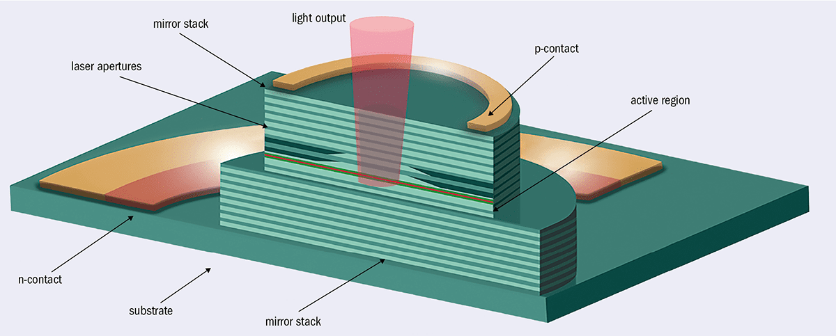
Most VCSEL production is in the infrared regime, typically between 850–940 nm for 3D sensing and slightly longer wavelengths for other applications. The production process begins by growing an epitaxial stack consisting of multiple layers of a compound semiconductor material such as gallium arsenide. Then you etch the device to define its dimensions (especially in the emitting region), oxidize part of the surface to define the laser aperture, and passivate – that is, protect against damage – the side walls. Finally, you do another etch to define the overall device size and make a contact on the negative or n-side of the device, which could be either the top or the back side. The light is emitted from the p-side of the VCSEL (see diagram below).
The individual steps in making a VCSEL – etching, deposition, and so on – are very similar to silicon chip manufacturing. However, the overall process is extremely simple in comparison, and the post-assembly steps are a lot more straightforward than for edge-emitting lasers. Because of the way they’re manufactured, VCSELs can easily be packaged into arrays, with hundreds of emitting regions on a single chip. That’s much more difficult to do with edge-emitting lasers.

If they’re relatively simple to make, why haven’t we seen more of them?
Until recently the applications – including 3D sensing, as well as active optical interconnects in the telecoms sector – were all relatively low-volume. What’s happened of late is that 3D sensing has emerged as a big trend in smartphones, starting with the front-facing image-recognition camera on Apple’s iPhone X. We’ve also heard that manufacturers of Android phones are poised to enter the market with similar capabilities.
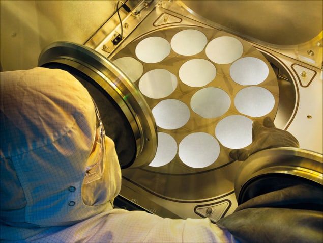
The moment you enter the smartphone market, the volumes become enormous. You’re talking about millions of units, potentially going to a billion units over time. That requires a completely different approach to manufacturing. For example, when you go from small semiconductor wafers to larger wafers, controlling wafer defects becomes much more important. VCSEL manufacturers are starting to adopt the practices of silicon fabs to make these devices in volume.
Why are VCSELs so well-suited for 3D sensing?
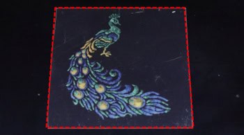
Traditionally, people have used LEDs for 3D sensing, but because light from an LED isn’t collimated there are limits to its effectiveness. With a laser, you get a collimated beam with a very narrow linewidth, and you can use multiple beams to map a surface. The device used on the iPhone X, for example, is called a dot projector, and it uses an array of VCSEL apertures on a chip to project a pattern of infrared laser light onto the object to be observed. That pattern is then recorded, and 3D information is created from the pattern in the form of a mesh. The whole process is extremely fast, and because the light is infrared it’s not intrusive. These attributes are significant benefits compared to alternatives such as cameras. Even if you use two cameras stereoscopically to create 3D information, you don’t get the spatial resolution you get with a VCSEL array.

What are the challenges of making VCSELs for this application?
The performance of the device is largely set by the epitaxial growth step, and the main thing you’re trying to achieve is extremely good wavelength control. You want to make sure that all the apertures are emitting uniformly, because if the object you’re trying to image is in bright sunlight, you have to apply a filter on your detector to distinguish between the sunlight and the light that’s being projected by the VCSEL array. The narrower you can make the filter, the more you can eliminate the ambient light. Today, a typical bandpass filter lets in a range of maybe 20–30 nm, and certain applications, such as LiDAR, need an even narrower range to be able to discriminate between signal and noise for objects that are far away. That’s the reason for tight wavelength control. Otherwise you’re wasting photons.
Another challenge, which I mentioned earlier, is controlling defects on the chip. This was less of an issue when chips were smaller and you could just throw away the ones that didn’t work, but if you have a large-area chip and all the apertures have to work for the chip to function, you have to make sure the defect rate is very low.
One source of defects on semiconductor wafers is the epitaxial growth process itself. You need good control of the material’s composition, so that you don’t get defects due to lattice strain between the semiconductor layers. Another source of defects is the parasitic deposition during the growth process. This can accumulate on the walls of the reactor, and if they flake off and fall onto the wafer, that’s a problem. At Veeco, we’ve improved our reactor design to make sure there’s no accumulation of unwanted material above the plane of the wafer.
Where do you see VCSELs being used in the future?
The next area, after smartphones, will be in automobiles, and there are two applications that people are working on in that sector. One is using cameras combined with VCSEL technology for in-cabin monitoring, keeping track of the driver or occupants within the car. The other is LiDAR. Autonomous cars need to “know” what’s around them, and LiDAR can do that, but today’s units are expensive, bulky and mounted on top of the car. They’re not aesthetically pleasing. It would be nice to replace them with an array of less obtrusive, cheaper sensors – the aim is below $100 per unit – that can map everything around the car and enable it to reach higher levels of autonomy. Level 5 autonomy, where a human driver never has to intervene, may not happen, but even at lower levels of autonomy, more sensors would improve safety.
The third application is in data communications. People are trying to push data speeds in optical fibres up to 50 gigabits per second, and VCSELs may help because better wavelength control means you can pack more wavelengths into a single fibre.
Overall, though, I like to make a comparison between VCSELs and light-emitting diodes. LEDs used to be a niche market too, until they got introduced as backlights in cell phones and TVs, and then into solid-state lighting. That was enabled by improvements in LED manufacturing, and particularly by better control of the epitaxial growth step. We think the same thing could happen in VCSELs, and that some of the technology we provide could bring similar benefits to VCSEL manufacturing as the industry positions itself for the next big ramp-up in production.


