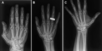
X-ray imaging plays a vital role within diagnostic medicine, with modalities such as radiography, fluoroscopy and computed tomography (CT) enabling visualization of the internal structure of the human body. But exposing the body to ionizing radiation comes with an associated risk, and the medical imaging industry is continually seeking new ways to reduce the required imaging dose, via sensitive, high-resolution detectors.
One emerging approach is to use lead halide perovskites to create high-sensitivity X-ray detectors. These materials contain heavy elements such as lead and iodine that have a large X-ray scattering cross section. And as they directly convert X-ray photons into an electrical signal, perovskites offer higher sensitivity and lower cost than competing scintillator-based detector technology. Integrating these perovskites into standard microelectronics, however, remains a challenge.
Now, researchers in Switzerland have demonstrated that 3D aerosol jet printing, a low-cost technique that deposits material with micron precision, can be used to build X-ray detectors from the perovskite methylammonium lead iodide (MAPbI3) on graphene. As they report in ACS Nano, the resulting devices exhibited a record sensitivity of 2.2 × 10⁸ μC/Gyair/cm2 when detecting 8 keV X-ray photons at low dose rates – four orders of magnitude higher than today’s best-in-class detectors.
“By using photovoltaic perovskites with graphene, the response to X-rays has increased tremendously,” says group leader László Forró, from EPFL’s Laboratory of Physics of Complex Matter, in a press statement. “If we would use these modules in X-ray imaging, the required X-ray dose for forming an image could be decreased by more than a thousand times, decreasing the health hazard of this high-energy ionizing radiation to humans.”
Device optimization
Halide perovskites such as MAPbI3 form elongated crystallites when dissolved in a polar aprotic solvent. During aerosol jet printing, as this solution travels through the nozzle, the crystallites grow and land on the substrate as crystalline nanowires containing little solvent. Once a droplet reaches the substrate, the solvent is mostly evaporated, reducing any spatter and creating the well-defined 3D structures needed to construct an X-ray photodetector with high spatial resolution.
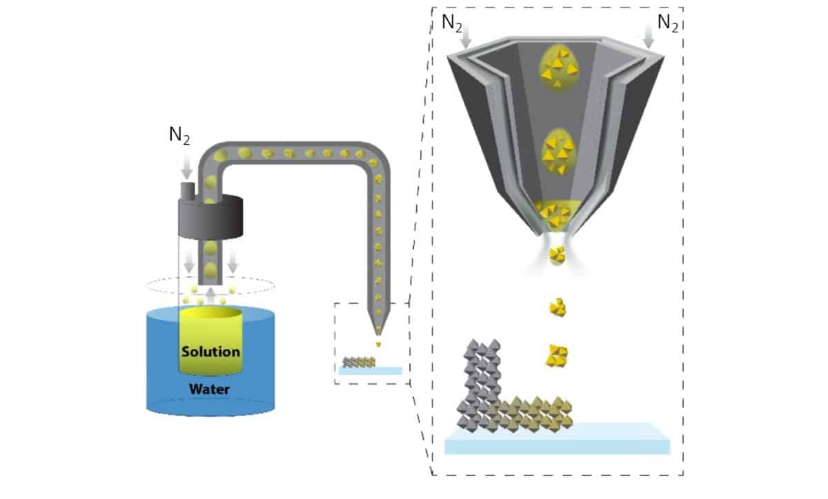
Using the aerosol jet printing device at CSEM in Neuchatel, the team first characterized the properties of different MAPbI3 geometries printed on microstructured silicon surfaces. A 3D-printed pillar showed an increased charge carrier collection compared with a 2D spot. Both 2D and 3D geometries enabled detection of low light intensities, down to 31.4 μW/cm2 under 650 nm illumination.
To further improve the photodetection characteristics, the researchers 3D-printed the perovskite on graphene, which amplifies the generated photocurrent. After testing several architectures and operation modes (resistor, diode and heterojunction) they found that the optimal pixel design was a heterojunction, with a MAPbI3 pillar printed on a graphene layer spanning the gold electrodes.
X-ray detection
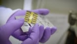
To create the X-ray photodetector, the researchers fabricated a sensing chip containing 3D-printed MAPbI3 walls of about 600 μm in height. They investigated the X-ray detection properties of the fully integrated detector by exposing it to an 8 keV X-ray source for 10 s at various dose rates. The X-ray detection limit was reached at a dose rate of 0.12 μGy/s, below which the signal could not be distinguished from the background noise. At the highest dose rate examined, 358 μGy/s, the device exhibited high photocurrents of up to 4000 μA/cm2.
As the sensitivity of the device is dose-rate dependent, the team determined its sensitivity at 100 mV bias for three dose-rate regions. The sensitivity of a detector pixel (with an estimated surface of 0.075 mm2) was largest at dose rates below 1 μGy/s, reaching 2.2 × 10⁸ μC/Gyair/cm2. Above 1 μGy/s, the photocurrent begins to saturate, yielding sensitivities of 2.5 × 10⁷ μC/Gyair/cm2 at up to 40 μGy/s, and 2.9 × 10⁶ μC/Gyair/cm2 from 40 to 100 μGy/s.
One obstacle preventing commercialization of perovskite-based optoelectronics is their stability. To protect the active MAPbI3 layer in their device, after wire-bonding, the researchers encapsulated the detector in a PDMS polymer. They note that the assembled detector unit was stable for over nine months, with no degradation in performance.
Thin-film perovskite detectors could enable extremely low-dose medical imaging
“We are confident that this X-ray detector unit architecture is extremely promising for highly sensitive X-ray imaging,” the researchers conclude. “This approach could allow significant lowering of the radiation doses required for X-ray imaging, resulting in safer and more affordable CT imaging systems.”
For medical imaging, the detector units will need to be assembled into a large surface area X-ray detector. The team also note that as CT scans use higher X-ray energies than the 8 keV source employed in this work, measurements should be repeated for 100 keV photons to confirm the device’s suitability for medical applications.