Paul Jorden describes how optical technologies that were developed for the astronomy market are making their mark in other fields
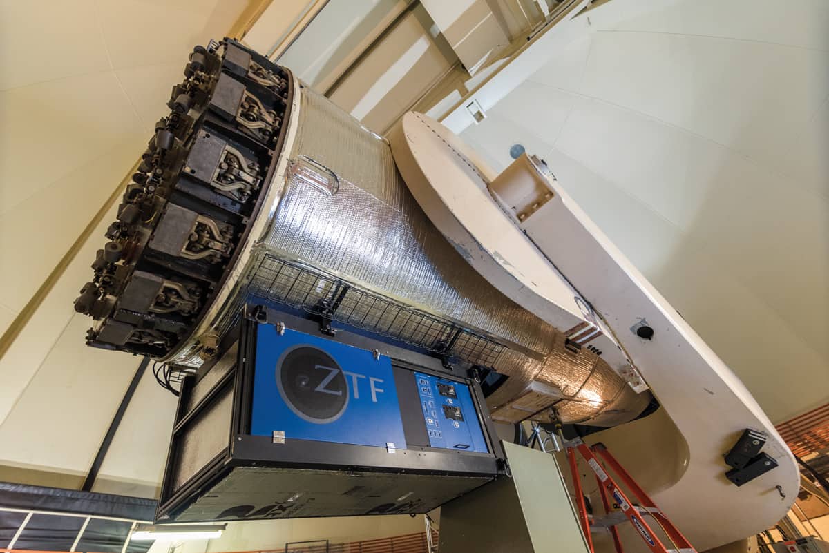
Telescopes and satellites are complex pieces of equipment, expensive to build and to operate. Consequently, astronomers and space scientists demand – and are prepared to pay for – sensors that maximize what they can achieve scientifically. Astronomers, especially, are looking at faint objects that are usually very far away, such as distant galaxies, stars and exoplanets. To capture light from these objects, they need telescopes with both large collecting areas and highly sensitive detectors.
One aspect of sensitivity is the quantum efficiency of the detectors – a measure of how well you can collect photons and use them. The other aspect is the noise associated with reading that photon signal into your system. A third important parameter is effectively the telescope’s operating efficiency, which depends on how quickly you can read out the sensors. These facilities may cost hundreds of thousands of dollars per night to run, so it is important that they spend most of their time capturing light and as little as possible transferring data into a computer.
These three requirements – high quantum efficiency, low noise and high operational efficiency – have long helped to drive improvements in detectors built for the astronomy market. More recently though, we are seeing the benefits of these improvements in areas outside astronomy as well. Here are a few examples.
Quantum efficiency
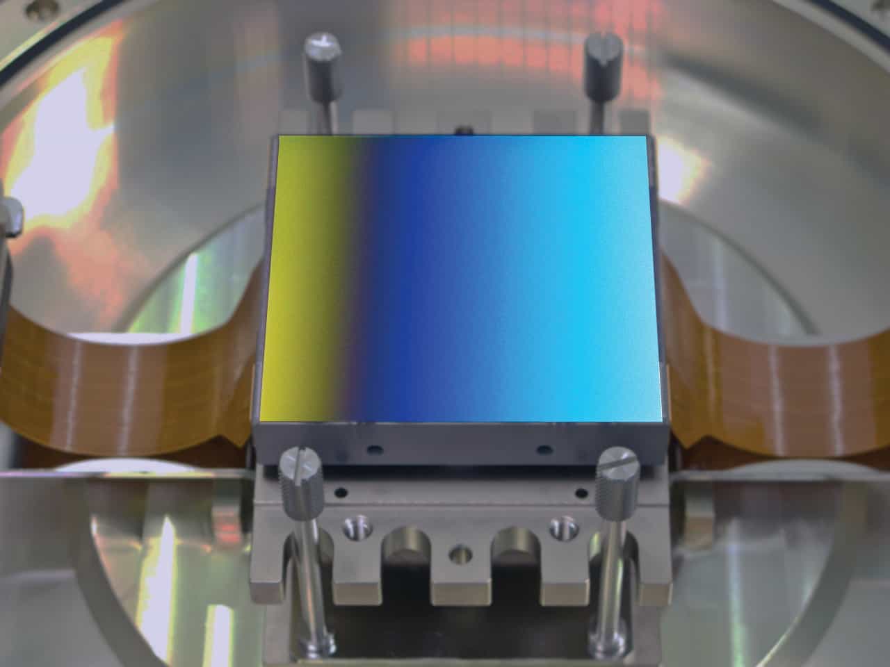
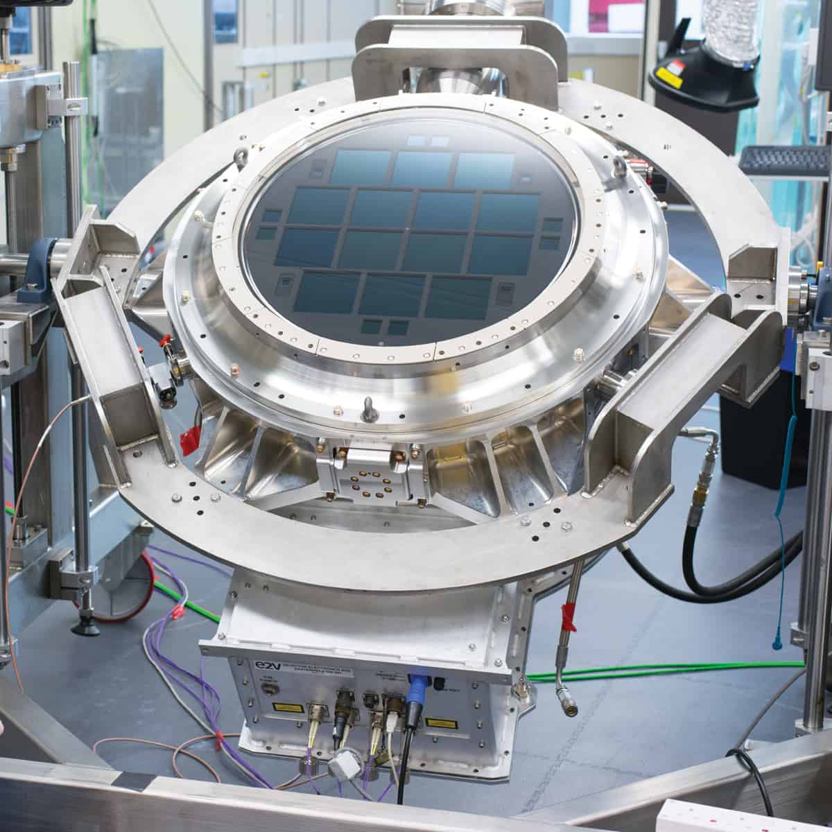
Silicon sensors have electrodes on their front surface. These electrodes are partly transparent, but even so, a “front illuminated” sensor is only around 50% efficient at recording photons. Since the 1980s, however, we have been able to remove most of the silicon material, tip the sensor upside down and illuminate it from the back side instead. This allows the photons to hit the silicon without any intervening layers, giving you very close to 100% efficiency. Back illumination also extends the wavelength range, making it possible to use sensors at soft X-ray and ultraviolet wavelengths to collect photons that would otherwise be absorbed in the surface layers of silicon.
Back-illuminated sensors are more expensive and time-consuming to make, but in the astronomy and space market that trade-off is worthwhile for all of the reasons mentioned above. More recently, though, this technology has become increasingly prevalent and valuable in other areas as well. For example, all modern mobile phones include CMOS sensors in their camera chips, and there is a huge drive to make these chips smaller. We are now at the point where the pixel size of the sensors is down to ~1 µm, and as the pixels shrink, their collecting area gets smaller, lowering their sensitivity. That’s a disadvantage, but within the last 10 years, manufacturers have begun to compensate by using back-illuminated technology. Back illumination is also becoming more common in sensors for other markets, such as drug discovery, DNA sequencing and life sciences more generally.
Red sensitivity
Many recent cosmological studies of dark energy and dark matter have involved measuring distant objects with very red-shifted light. However, chips made with standard materials, designs and processes have only a modest red sensitivity. There is a good reason for this: the response of the human eye begins to roll off at wavelengths in the near-infrared, so if you are making a chip for a digital camera, you probably want it to have a similar sensitivity. But astronomers need to measure all wavelengths, so at Teledyne e2v we have developed techniques (such as making the silicon thicker so that it absorbs near-infrared light better) for making our sensors more red-sensitive.
We have supplied these sensors to the astronomy market for a long time, but red sensitivity is also starting to be advantageous in sensors used in ophthalmology thanks to a technique called optical coherence tomography. This technique uses near-infrared illumination to penetrate a little bit deeper into cells, so red-sensitive sensors have obvious benefits.
Adaptive optics
The basic purpose of adaptive optics is to correct for the turbulence and disturbance caused by the Earth’s atmosphere. This doesn’t apply to space telescopes, of course; once you’re up there, you don’t have to look through air. But all ground-based astronomers do, even if they’re high up a mountain, and that imposes a limit on how sharp their images can be.
To fix this, you need to point the telescope at a “reference star” of some sort, measure the wavefront coming from the reference star, capture it with a wavefront-sensing detector, read out the detector in 1–10 ms, and feed the signal into a closed-loop system with a deformable mirror that essentially corrects for what the atmosphere has done. The result is an image that will be sharper than it would have been without the technique.
At the moment, we are working on an adaptive-optics system for the Extremely Large Telescope (ELT), which is under construction for the European Southern Observatory on their telescope in Chile. The ELT is a 39 m diameter telescope that will cost about €1bn and will be the largest telescope in the world when it’s finished in 2024, but without adaptive optics it would be no better than smaller, older instruments built a generation or more ago.
The usefulness of adaptive optics is not limited to astronomy. There are also some emerging applications in laser communications – for example, in optical communications between ground and satellite – and medical applications are becoming more widespread. For example, if you want to capture images of the human retina, you can build a very-high-resolution microscope, but when you use it to look through the front of the eye, the cornea and the lens will disturb the sharpness of the retinal image. Clinicians want to see the blood vessels, the structure, and even the photoreceptors – the cones and rods – in the retina. To do that they are starting to use adaptive-optics instruments that can correct, 100 times a second, for the modulations or imperfections of the eye. It’s a powerful technique, and it is not limited to big research instruments anymore: it is also used in the medical diagnostics found in hospitals.
Multispectral imaging
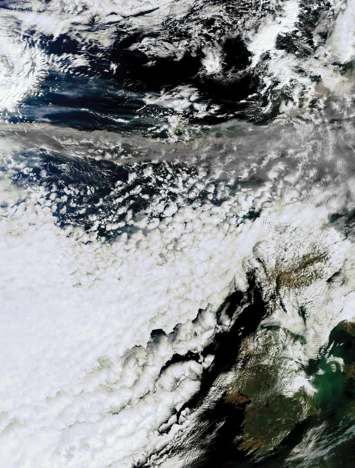
Astronomers have always wanted to make measurements with spectrographs that cover as large a wavelength range as possible. That kind of spectral range used to be much less common for instruments that look down from satellites to the Earth, but now there are many hyperspectral satellites up there scanning the atmosphere, the sea or the land. These newer satellites use more complex sensors than the old broadband filters, and that means they can get good spectral resolution and good spatial resolution at the same time. Because of this, they can distinguish, for example, how well trees are growing, what type of foliage is in an image or what types of minerals are on the Earth’s surface. With broadband filters, you can get some of that information, but it’s rather crude.
This technology is now being extended to less expensive instruments. It’s being used on drones, for example, that fly over farmland to conduct agricultural surveys, and in food processing, where you might use it to detect whether your potatoes have a fungus. With high-resolution spectral information you can really see what the problem is, as opposed to just detecting a slight change in colour.
Curved sensors
For most optical systems – including our own eyes – the focal surface is either spherical or curved. Despite this, essentially all sensors that have ever been made commercially are flat. This is because when you make sensors, you typically start off with a silicon wafer that has been polished so flat that you can see your face in it, and all the manufacturing equipment is designed to operate with a flat wafer. For example, the big, expensive optical lithography machines that project patterns onto silicon to create the structure of the circuit will only focus properly if the surface of the wafer (150–200 mm across) is flat to a precision of 1 µm, This means that the finished devices are only flat and cannot be curved when first made. However, there is a lot of development work being done on technologies that allow you to curve flat wafers after they have been made. This is difficult to do because silicon is a crystal and it doesn’t like being bent – you impose stresses in it when you bend it – and we are now learning the limits of how much you can do that and still have it function in an imaging system.
There is a lot of interest in making curved detectors or sensors because it would reduce the number of optical elements in a system. At the moment, when people design imaging cameras or spectroscopic instruments, they have to put in extra optical elements to focus the light onto a flat detector. Those elements cost money, take up space and introduce both extra complexity and some degradation in design quality. On the ELT, for example, some instruments are the size of an entire room and the optical elements are correspondingly large. If you could cut out a few of them, you could save millions. The same principle applies for space-based instruments, where cutting out optical components would give you a better system that is also smaller and lighter.
Space agencies are paying for the development of these technologies because they can see their benefits, but other, more “down to Earth” companies – Sony, Apple, Microsoft and others – are also starting to do research on curved sensors. As with back-illuminated sensors, the driver here is the miniaturization of mobile-phone technology. If you want to make a small camera for a mobile phone, you generally have to put a tiny lens (or multiple lenses) in front of it. A curved sensor would make the optics of these cameras simpler. For example, to make a compact camera with a wide field of view – like a fish-eye camera – you need a huge and difficult-to-manufacture piece of shaped glass to make a lens that will accomplish that with a flat detector. But if you can make the detector curved, the components in front of it can get smaller and cheaper, and so can the device as a whole.
And one for the future
One thing that we are seeing now is a transition from CCD technology to CMOS technology. These are both silicon technologies, and if you had asked me 20 years ago what an astronomer would need, the answer would probably have been CCDs. But the chips in mobile phones are CMOS-based, and we are now making more and more CMOS devices for use in both ground-based and space-based astronomy. CMOS chips have several advantages for astronomy and space applications. One is that they are “harder” against radiation – they tolerate being irradiated better than CCDs. They are also more integrated in the circuitry that’s inside them, so they are easier to operate and you don’t need as many other electronics around them to get the data out and back to wherever you’re storing it.
Overall, we see two pulls for the types of technology development we do. One pull comes from customers, and curved sensors are a good example – various people have asked for that, so we are working on it. But the other pull is our internal knowledge of what’s possible. We create a road map of technology developments each year, and curved sensors, new CMOS sensors and improved wavelength sensitivity are all on it. We are pushing the boundaries as much as we can all the time, because as astronomers know well, nothing in this field ever stands still.