By combining the best optical properties of inorganic and organic waveguides in a hybrid chip, researchers at the Chalmers University of Technology in Sweden demonstrate evanescent-wave microscopy using just a conventional microscope. The development allows low-cost and low-energy fabrication of a waveguide that can make imaging of biomaterials more accessible.
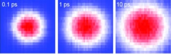
Traditionally, evanescent-wave microscopy is carried out using a total internal reflection fluorescence (TIR) microscope. In such a microscope, scientists produce a thin slither of “non-propagating” evanescent light that hovers just above the sample surface and allows observation of surface-bound fluorophores, which is useful in the study of molecular interactions such as cell adhesion, protein binding, and hormone binding. Using evanescent light for these observations limits the amount of background signal compared with what scientists typically observe in conventional fluorescence microscopy. Still, however, the area of illumination is small, the penetration depth of the light is limited to around 200 nm, and the method is totally reliant on the use of fluorescent material for signal generation.
The waveguide developed by the researchers at Chalmers eliminates the need for costly TIR microscopes and allows for nanoscopic objects to be detected without the use of fluorescent labels. The waveguide only requires the use of a conventional light microscope combined with a fibre-coupled laser and generates an evanescent wave with an improved penetration depth of below 100 nm. The penetration depth can also be varied by tailoring the thickness and refractive index of the core-layer of the slab.
“The design and fabrication is rather simple and straightforward compared to most nano-devices out there,” said co-author Bjorn Agnarsson, a post-doctoral fellow in the Department of Physics. The biggest challenge in development was keeping the surface of the waveguide’s core layer flat and free of contaminates to ensure the structural integrity of the fabricated chip. Now, however, using the fabrication technique detailed in the paper published in Nano Futures, the team can easily fabricate 100 chips within a few days.
Super resolution microscopy gets a dose of deep learning

Tailoring to task
According to co-author Mattias Sjöberg, a PhD student in the Department of Physics, the device can be tuned to different applications simply by changing the material of the device’s cladding layer. Since their team is interested in biological applications where molecules are in aqueous environments, they chose cyclized transparent optical polymer (CYTOP), a polymer that has the same refractive index as water.
“CYTOP allows for reduction of stray light, which is an advantage that other devices don’t have,” said Sjöberg. “Plus, we significantly reduce costs since we don’t need to use specially designed TIR microscopes and objectives.”
With their device optimized, next the team plans to look at using it for label-free studies of the interactions between proteins and biological nanoparticles such as vesicles.