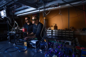
Researchers in the US have shown how light travelling through optical waveguides can be converted into freely propagating light waves with arbitrarily shaped wavefronts – an achievement that the team claims as a first. Nanfang Yu and colleagues at Columbia University and at the City University of New York (CUNY), achieved the feat using “leaky-wave metasurfaces”.
Although there are many different optical systems for controlling light, they tend to fall into two types. One involves controlling the properties of light waves travelling through free space, and can include systems ranging from simple lenses, to advanced telescopes and holograms. The other type involves the use of photonic circuits, which manipulate light propagating along optical waveguides with a cross-sectional dimension of typically hundreds of nanometres. These circuits are ideal platforms for optical information processing, making them key elements of modern devices including sensors and optical communications chips.
With advances in optical technologies ranging from augmented reality, to probes for controlling and manipulating neurons, there is growing motivation to integrate these two categories of optical control systems. Yet as Yu explains, the two have so far remained largely incompatible with each other.
Interfacing challenges
“There has always been a challenge in ‘interfacing’ these two categories,” he says. “It is fundamentally hard to transform a tiny and simple waveguide mode into a broad and complex free-space optical wave, or vice versa. However, demands for ‘hybrid’ systems consisting partly of photonic integrated circuits and partly of free-space optics are becoming real.”
For Yu and colleagues, the solution lies with metasurfaces, which are thin sheets made from arrays of sub-wavelength sized structures. These metasurfaces can alter the properties of light waves passing through them. In their previous research, they showed how metasurfaces can be used to manipulate light travelling in free space.
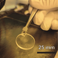
To extend these capabilities to guided light waves, the researchers started with a photonic crystal (PhC) comprising a square array of square holes in a polymer film. This PhC allows flat sheets of light to propagate back and forth as standing waves.
Symmetry-breaking perturbation
“In the next step, we introduced a symmetry-breaking perturbation to the PhC slab by deforming square holes of the PhC into rectangular ones,” Yu explains. “The perturbation lowers the degree of symmetry of the PhC so that the photonic modes are no longer confined to the slab and can leak into free space, with a leakage rate proportional to the magnitude of the perturbation.”
The team found that by varying the perturbation across the slab – orienting its rectangular holes along different directions – they could fine-tune the shape of the wavefront of the leaking light. Using their leaky-wave metasurfaces, Yu’s team developed a new technique for converting the light propagating through a waveguide into a wave travelling in free space.
Reconfigurable metasurface steers incoherent light in less than a picosecond

“Here, an input waveguide mode is first expanded into a slab waveguide mode, which enters a leaky-wave metasurface and produces the desired surface emission,” CUNY’s Adam Overvig explains. “In this way, the initial simple waveguide mode confined within a waveguide with a cross-section on the order of one wavelength is eventually converted into a freely propagating light wave with a complex wavefront, over an area about 300 times of the wavelength.”
The team demonstrated how their devices could produce diverse emission patterns. These included 2D arrays of focal spots, corkscrew wavefronts, holographic images, and laser beams with spatially varying polarizations. If the technology is scaled up, these could one day be applied across many different types of advanced optical systems. Applications include optical displays like holograms and augmented reality goggles; and high-capacity optical communication channels between computer chips.
In quantum optics, optical lattices are used for trapping ultracold atoms and molecules. “Compared to traditional methods where optical lattices are produced by interference of multiple beams via free-space optics, our devices could be directly integrated into the vacuum chamber to simplify the optical system, making portable quantum optics applications such as atomic clocks a possibility,” Columbia’s Heqing Huang explains.
The research is described in Nature Nanotechnology.