A single layer of silver and tellurium atoms (AgTe) has been grown on the (111) facet of a silver substrate (Ag(111)) for the first time ever. Little is known about this material other than that its electrons experience strong spin-orbit coupling, which could lead to novel and potentially useful electronic properties. This development happened by chance, when researchers in China were attempting to grow the promising topological insulator candidate, 2D Ag2Te.
New and interesting 2D materials have been sought by physicists ever since the discovery of freestanding graphene about 15 years ago. This search has yielded silicene, germanene, phosphorene and other materials with atoms adjacent to the diagonal line on the periodic table that connects boron and astatine. It is no surprise, therefore that scientists are now looking for potential 2D materials containing tellurium.
Recently, a theoretical study suggested that a 2D Ag2Te crystal could be a topological insulator at room temperature. Most known 2D topological insulators require very low temperatures so such a material would be an ideal candidate for use in energy-efficient electronic and spintronic devices that make use of topological materials. And so a research team at the University of Chinese Academy of Sciences, Beijing, China, took it upon themselves to try and grow a 2D monolayer Ag2Te onto a Ag(111) substrate.
A nice surprise
The researchers used molecular beam epitaxy in ultrahigh vacuum onto an atomically flat substrate. They used a scanning tunnelling microscope (STM) to identify regions in the monolayer that had distinct patterns. One region resembled a flat honeycomb structure with periodic buckled ridges. As they had expected monolayer Ag2Te to be hexagonal, this was the first clue that they had grown AgTe instead. Team member Geng Li, said that discussions with several epitaxy experts confirmed their suspicion. “Scientific research often gives people surprises, which are not always bad”, comments Li.
AgTe is even less studied than Ag2Te and this is the first time it has been fabricated in a monolayer. It is known, however, to have strong spin-orbit coupling, so Li is optimistic about its potential for having interesting physical properties. The researcher also speculates that “the buckled honeycomb structure may have anisotropic electronic or thermal transport properties” if isolated from the substrate.
The origin of the buckled structure is unclear, and it has not been seen in monolayer copper selenide (CuSe), which is expected to be similar to AgTe. The researchers, however, strongly suspect that it arises in order to relieve some of the strain from the substrate-monolayer lattice mismatch. This is also the expected origin of another observed region, which has a striped pattern. In this region the honeycomb is stretched along one direction and forms stripes that resemble a Moiré pattern.
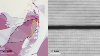
The team also tried increasing the tellurium dosage onto the substrate, which resulted in a spotted-pattern structure. Multiple holes appeared throughout the general honeycomb lattice (see figure) – with silver and tellurium atoms removed from the lattice to strengthen the overall structure. Such a pattern has also been seen in cerium selenide (CeSe). All these phenomena – lattice distortions and formation of holes – are related to strain in the thin film.
The first-time fabrication of a new and unstudied 2D material is an exciting development for Li and colleagues, who have already started work on investigating the electronic properties of the monolayer, but Li reminds that it is still early to talk about potential applications. And the researchers have not given up on trying to grow monolayer Ag2Te and Li says that they are considering other inert substrates and growing conditions.
Full results reported in Chinese Physics Letters.